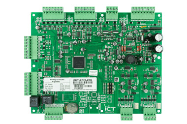
The mainstream circuit board assembly technology in the SMT industry should be full-flow reflow soldering,is divided into single-panel reflow and double-panel reflow.
Which SMD parts should be placed on the first side of the reflow oven?
Generally speaking, the smaller parts are recommended to be placed on the first side of the reflow oven, because the deformation of the PCB will be smaller when the first side passes through the reflow oven, and the precision of solder paste printing will be higher, so it is more put small parts.
Second, the smaller parts do not risk falling down during the second reflow oven. Because the first surface part will be placed directly on the bottom surface of the circuit board when facing the second side, when the board enters the high temperature of the reflow area, it will not fall off the board because of excessive weight.
Third, the parts on the first panel must pass through the reflow furnace twice, so the temperature resistance must be able to withstand the temperature of two reflows. The general resistance and capacitance are usually required to be reflowed at least three times. In line with the requirements of some boards, it may be necessary to go back to the soldering furnace again because of the maintenance relationship.
Which SMD parts should be placed on the second side of the reflow oven?
Large components or heavier components should be placed on the second side to avoid the risk of parts falling into the furnace when the furnace is over.
LGA and BGA parts should be placed on the second side of the furnace as much as possible. This avoids the risk of unnecessary re-soldering during the second pass to reduce the chance of empty/false welding. If there are small and small BGA parts, it is not recommended to place them on the first side of the reflow oven.
Parts that cannot withstand too much heat should be placed on the second side of the reflow oven. This is to prevent the parts from being damaged by too many high temperatures.
PIH/PIP parts should also be placed on the second side of the furnace unless the length of the solder fillet does not exceed the thickness of the board, otherwise the foot protruding from the surface of the PCB will interfere with the steel stencil on the second side, which will make the second side solder paste printed steel stencil can not be flat on the PCB, causing abnormal solder paste printing problems.
Some components may have soldering inside. For example, a cable connector with an LED lamp must pay attention to whether the temperature resistance of the component can pass through the reflowing furnace twice. If it is not possible, it must be placed on the second surface.
Some components may have soldering inside. For example, a cable connector with an LED lamp must pay attention to whether the temperature resistance of the component can pass through the reflowing furnace twice. If it is not possible, it must be placed on the second surface.
In addition, in the mass production of electronic components to be soldered to the PCB board, there are many ways, but each process is actually determined at the beginning of the board design because its board The placement of the parts will directly affect the welding sequence and quality of the assembly, while the wiring will have an indirect effect.
At present, the welding process of the circuit board can be roughly divided into full-plate welding and partial welding. The full-board welding is roughly divided into reflow soldering and wave soldering, while the board is partially soldered with carrier wave soldering, selective wave soldering, laser soldering,etc.


