Categories
PCB Blog

What documents should be provided for PCBA quotation?

What documents should be provided for PCBA quotation?

The information to be provided for PCBA processing is gerber file (production data Of PCB board) and bom list (material list or component list).The English name is Bill Of Material. It should be noted that the list of components should be as clear and detailed as possible, including the brand, specification, size, quantity and type of components etc.

What are the common types of PCBA substrates?

1. FR-4 sheet is an epoxy board with high mechanical and dielectric properties, good heat resistance and moisture resistance, and good mechanical processing.

2. The aluminum substrate is a metal-based copper clad laminate with good heat dissipation function. Generally, the single panel is composed of a three-layer structure, which is a circuit layer (copper foil), an insulating layer and a metal base layer. Aluminum substrates are commonly used in LED lighting products.There are two sides, the white side is the welding LED pin, and the other side is the color of aluminum, which will contact with the thermal conductivity after applying thermal coagulation.

3. The FPC board is a highly flexible and excellent flexible printed circuit board made of polyimide or polyester film. It has the characteristics of high wiring density, light weight, thin thickness and good bending characteristics.Used in high-end products such as mobile phones and hard drives.

Depending on the product application, the choice of PCBA substrate will be different. Generally, the more high-end products are, the more advanced PCBA substrates are and the more expensive they are.

PCBA storage conditions and requirements?

(1) conformal coating
For a long time not used PCBA board, should be coated with conformal coating,which has the functions of moisture-proof, dust-proof and anti-oxidation, which can effectively extend the storage time and extend the time after applying conformal coating for 9 months.

(2) vacuum packaging
PCBA storage is not in contact with air and water. Firstly, the PCBA board is packaged in a vacuum bag, and the edge of the box needs to be surrounded with a layer of bubble film when packing.The bubble film has better water absorption, which plays a very good role in moisture-proof. Of course, moisture-proof beads are also indispensable.Then sort the emissions and label them.After the box is sealed, the box must be separated from the wall, stored in a dry and ventilated place, and avoid sunlight.

(3) control the temperature and humidity of the warehouse
The temperature of the warehouse where PCBA is stored is preferably controlled at 23±3°C, 55±10%RH,the storage temperature is less than 25 degrees, the relative humidity is less than 65%, with temperature control and no corrosive gas in the indoor environment.For the OSP process PCB, due to its thin protective film, PCBA requires more stringent storage conditions for storage.

Categories
PCB Blog

What is the meaning of Multi-layer in PCB Board?

A PCB board is a printed circuit board. A multilayer PCB is also a multilayer circuit board, also called a multi-substrate board.

The increased density of integrated circuit packages leads to a high concentration of interconnections, which makes the use of multisubstrate necessary.Unexpected design problems such as noise, stray capacitance, crosstalk, etc. have arisen in the layout of printed circuits.Therefore, PCB design must focus on minimizing the length of signal lines and avoiding parallel lines.Obviously, in a single panel or even a double panel, these requirements cannot be answered satisfactorily due to the limited number of crossings that can be achieved.In the case of a large number of interconnection and cross requirements, the board to achieve a satisfactory performance, the board layer must be expanded to more than two layers, so there are multilayer PCB board.Therefore, the original intention of making multilayer circuit boards is to provide more freedom for complex and/or noise-sensitive electronic circuits to choose suitable routing paths.A multilayer circuit board has at least three conductive layers, two of which are on the outer surface, and the remaining layer is synthesized in an insulating plate.The electrical connection between them is usually made through a hole in the cross section of the circuit board.Unless otherwise specified, multilayer printed circuit board, like a double panel, is typically a plated through hole plate.

A multi-substrate is fabricated by stacking two or more circuits on each other with reliable pre-set interconnections. Since drilling and electroplating have been completed before all the layers have been rolled together, this technique has violated the traditional manufacturing process from the beginning. The innermost two layers are made up of traditional double panels, while the outer layers are different, they are made up of separate single panels. Before rolling,the inner substrate will be drilled, through-hole plated, patterned transferred, developed, and etched. The outer layer to be drilled is a signal layer that is plated in such a way as to form a balanced copper ring at the inner edge of the through hole. The layers are then laminated together to form a multi-substrate that can be interconnected using wave soldering (between components).

Rolling may be done in a hydraulic press or in an overpressure chamber (autoclave). In the hydraulic press, the prepared material (for pressure stacking) is placed under cold or preheated pressure (high glass transition temperature material is placed at a temperature of 170-180 °C). The glass transition temperature is the amorphous region of the amorphous polymer (resin) or portion of the crystalline polymer that changes from a hard, relatively brittle state to a viscous, rubbery temperature.

Multi-substrate is put into use in professional electronic equipment (computers, equipment), especially in the case of weight and volume overload. However, this can only be achieved by increasing the cost of the multi-substrate in exchange for space increase and weight reduction. Multi-substrate is also very useful in high-speed circuits, which provide designers of printed circuit boards with more than two layers of boards to route wires and provide large ground and power areas.

What are the advantages of multi-layer PCB boards?

The multi-layer circuit board is as the name suggests that more than two layers of boards can be called multi-layer. Before you analyzed what is a double-sided board, then the multi-layer board is more than two layers, such as four layers, six layers, eight layers and so on..Of course, some designs have three or five layers of circuit, also called multilayer PCB.The conductive trace diagram is larger than the two-layer board. The layer is separated from the layer by an insulating substrate. After each layer is printed, the layers are overlapped by pressing. After drilling, the vias are used to achieve conduction between each layer of the line. The advantage of a multi-layer PCB board is that the lines can be distributed in multiple layers of wiring, allowing for the design of more sophisticated products. Or smaller products can be achieved with multi-layer boards. Such as: mobile phone circuit boards, micro projectors, voice recorders and other volumetric products.In addition, multiple layers can increase the flexibility of design, which can better control differential impedance and single-end impedance, as well as better output of some signal frequency.

Multi-layer printed circuit is rapidly developing towards the direction of high density, high precision and high level digitization.Because of the need for high-speed circuits in the computer and aerospace industries.It is required to further improve the packaging density, and with the reduction of the size of the separated components and the rapid development of microelectronics, the electronic equipment is developing towards the direction of reduction in size and quality.Due to the limitation of available space, it is impossible to improve the assembly density further.Therefore, it is necessary to consider using more printed circuits than the number of double panel layers.This has created the condition to the multilayer pcb circuit board appearance.

Categories
PCB Blog

PCBA Production Process and Equipment Introduction

1. solder paste printing machine
Modern solder paste printing machines are generally composed of plates, tin paste, embossing, and transmission boards. Its working principle is: firstly, the circuit board to be printed is fixed on the printing positioning table, and then the solder paste or the red glue is printed on the corresponding pad through the steel mesh by the left and right scrapers of the printing machine, and the PCB which is uniformly printed is passed through. The transfer station is input to the placement machine for automatic placement.

2. placement machine
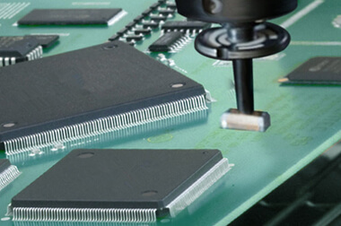
Mounter: Also known as “mounting machine” or “Surface Mount System”, in the production line, it is placed behind the solder paste printer, and the surface mount components are accurately placed by moving the head. Place a device on the PCB pad. Divided into manual and fully automatic.

3. reflow soldering
Inside the reflow soldering there is a heating circuit that heats the air or nitrogen to a sufficiently high temperature and blows it onto the board that has been attached to the component, allowing the solder on both sides of the component to melt and bond to the main PCB board. The advantage of this process is that the temperature is easy to control, oxidation is avoided during the welding process, and manufacturing costs are easier to control.

4. component shearing machine
Used to cut and deform pin components.

5. wave soldering
Wave soldering is to let the welding surface of the plug-in board directly contact with high temperature liquid tin to achieve the purpose of welding, its high temperature liquid tin maintains an inclined surface, and by a special device to make the liquid tin form a wave like phenomenon, so called “wave soldering”, its main material is solder bar.

6. tin furnace
In general, a tin furnace refers to a welding tool used in electronic welding. For the discrete component circuit board welding consistency, easy to operate, fast, high efficiency, is a good helper for the production and processing.

7. washing machine
Used to clean the PCBA board to remove residue from the soldered board.

8. AOI detector
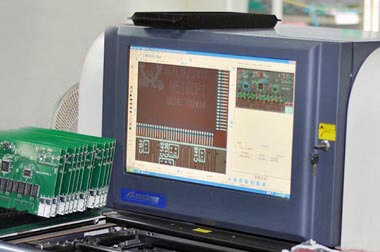
The full name of AOI is automatic optical inspection, which is used to inspect welding defects.AOI is a new emerging testing technology, but the rapid development, many PCBA manufacturers have launched AOI testing equipment.When automatic testing, the machine will scan PCB automatically through the camera, collect images, and compare the tested solder joints with the qualified parameters in the database. After image processing, the defects on PCB will be checked, and the defects are displayed/marked through the display or automatic signs for maintenance personnel to repair.

Categories
PCB Blog

In the PCBA processing, how does the program “burn” into the IC chip?

In PCBA processing, in order to achieve the expected specific functions of the board, in addition to hardware, software support is required. If you have software, you need to add the “burn” program in the PCBA processing process – “handle” the program into the IC.

Definitions:
The process of “handling” the program into the internal storage space of the chip is called burning.

Classification:
Burning methods are generally divided into offline burning and online burning.

1. Offline burning:
By connecting the adapter to the chip in different packages, the chip can be used with the adapter to achieve program burning. The nature of the adapter is similar to a precision fixture, and different packages of chips need to be mated with different adapters. If there is an error in the production test and the production backtracking is re-corrected, the chip needs to be detached from the adapter and re-recorded according to the prescribed process, which requires a large amount of manpower and material resources and a high cost. There are some unexpected situations when the PCBA is processed and produced. If the temperature of the circuit board is not high enough, the chip will be deformed when the chip is removed, which increases the risk of scrapping.

2. Online burning:
Online programming uses the standard communication bus of the chip, such as USB, SWD, JTAG, UART, etc. The interface is generally fixed, and there are few pins to be connected during programming. Since the interface communication rate is not high, the general cable can be used for burning without high consumption. Online burning is performed by wire connection. If an error occurs during the production test, the PCBA can be traced back and the burned can be performed again without disassembling the chip. Not only saves production costs, but also increases the efficiency of burning.

Categories
PCB Blog

SMT Manufacturing Process – First Piece Mechanism

In the SMT production process, there is a common error-proofing method, which can reduce the risk of wrong parts, reduce the probability of errors, and effectively improve the quality of the entire production. This is the first mechanism.

The so-called first piece mechanism is to make a sample before the official production. This board will be tested in all aspects. After all the tests have been passed, the official production will begin. The first piece is usually done under the following conditions: 1.The beginning of each work class; 2. Replace the operator; 3. Replace or adjust the equipment, process equipment (replace the SMT stencil, replace the model) 4. Change the technical conditions, process methods and process parameters 5.Use new materials or or material replacement (such as material changes during processing, etc.).

A reasonable first-piece mechanism can ensure that the components waiting to be installed on the placement machine are correct, the solder paste state used and the furnace temperature are all right. Can effectively prevent the occurrence of batch defects. The first-piece mechanism is a means to pre-control the production process of the product, an important method for product quality control, and an effective and indispensable method for enterprises to ensure product quality and improve economic efficiency.

Long-term practical experience proves that the first inspection system is an effective measure to detect problems early and prevent products from being scrapped in batches. Through the first piece inspection, system problems such as serious wear of the fixture or installation positioning error, deterioration of the measuring instrument accuracy, misreading drawings, feeding or formulation errors can be found, so as to take corrective or improvement measures to prevent the occurrence of batch unqualified products.

The following are some common methods for the first test. According to different production requirements, companies usually choose different test methods. Although the methods used are different, the final effect is the same.

1. The first test system is a complete set of integrated system, which can directly input the produced product BOM into the system. The test unit that comes with the system will automatically test the first sample and check the input BOM data. Confirm that the first prototype produced meets the quality requirements. The system is convenient and the test process is automated, which can reduce the error test due to personnel factors.Labor costs can be saved, but the initial investment is large. Now there is a certain market in the SMT industry and it has been recognized by certain enterprises.

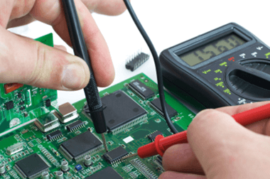
2. LCR measurement, this test method is suitable for some simple circuit boards, the components on the circuit board are reduced, there is no inheritance circuit, only some circuit boards of the components do not need to be returned to the furnace after the end of the injection, and the LCR is directly used. Measure the components on the board and compare them with the rating of the components on the BOM. If there is no abnormality, you can start production. This method is widely used by many SMT plants because of its low cost (as long as it can be operated with one LCR).

3. AOI test, this test method is very common in the SMT industry, suitable for all circuit board production, mainly through the shape characteristics of the components to determine the soldering problem of the components, but also through the color of the components, IC Check the silk screen to determine if there are any wrong parts in the components on the board. Basically, one or two AOI devices are standard on every SMT production line.

4. Flying probe test, this test method is usually used in some small batch production, which is characterized by convenient test, strong program variability, good versatility, and basically can test all types of circuit boards. However, the test efficiency is relatively low, and the test time per board will be very long. This test needs to be carried out after the product has passed through the reflow oven, mainly by measuring the resistance between the two fixed points to determine whether the components in the board are short-circuited, empty-welded, and wrong.

5.ICT test, which is usually used in mass PCB Assembly production machines, and the production volume is usually large and the test efficiency is high, but the manufacturing cost is relatively high,and each type of circuit board needs special fixtures. The life of each set of fixtures is not very long, and the test cost is relatively high. The test principle is similar to the flying probe test. It is also to measure the resistance between two fixed points to determine whether there are short circuits, empty welds, and wrong parts on the circuit components.

6. Functional test, this test method is usually used on some more complicated PCB circuit boards. The circuit board to be tested must be simulated after the soldering is completed, through some specific fixtures, to simulate the official use of the circuit board.In this simulated scenario, observe whether the board can be used normally after turning on the power. This test method can very accurately determine whether the board is normal.But there are also problems in that the test efficiency is not high and the test cost is high.

7.X-RAY inspection, for some boards with BGA package components, the first part of the production needs X-ray inspection, X-ray has strong penetrability, is the earliest used for various inspection occasions. An instrument with an X-ray perspective showing the thickness, shape and weld quality of the solder joints, and solder density. These specific indicators can fully reflect the welding quality of the solder joints, including open circuit, short circuit, holes, internal bubbles and insufficient amount of tin, and can be quantitatively analyzed.

Categories
PCB Blog

SMT Production Process for Electronic Circuit Board

With the development of miniaturization and thinning of electronic products, many pcb circuit boards in electronic products are now using SMT manufacturing technology, namely surface mount technology, that is, all electronic components are welded on the surface of circuit boards.There is no need to insert it through the reserved holes in the circuit board and weld it on the back as before.

SMT technology can make the production process of circuit boards more automated, faster, and less human intervention. Moreover, the components used in this technology have the advantages of smaller size, lighter weight, and more reliable than previous plug-ins.

An SMT production line includes the following main parts: printing presses, placement machines, reflow ovens, cooling equipment, and some auxiliary optical inspection equipment, cleaning equipment, drying equipment, and material storage equipment.