Categories
PCB Blog

KingPCB, the best Aluminium PCB manufacturer

Aluminium PCB manufacturer:  All You Need to Know


Finding the right Aluminium PCB manufacturer requires basic knowledge of Printed Circuit Boards itself. There are several types of printed circuit boards available, each serving either similar or different purposes.

The type of PCB you choose mainly depends on your electronic product requirement. Our objective today is to discuss one of the leading types of printed circuit boards, aluminium PCBs.


What is Aluminium PCBs


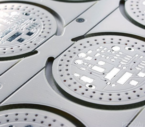
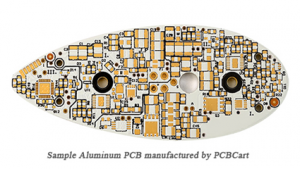
Aluminium Printed Circuit boards or commonly known as aluminium clad, metal-clad PCBs, aluminium base or insulated metal substrates transfer heat via a thin layer of conductive dielectric material.

Electrically insulating dielectric, yet thermally conductive is present between the copper foil and a metal base. The layer is extremely thin.In terms of the Printed Circuit Board, we would say that is a lamination of the layer between copper foil and metal base.

Aluminium PCB manufacturers etch the copper foil into their desired circuit patterns. This allows the metal to draw heat away from the circuit via t dielectric which is very thin.


aluminium-pcb-manufacturer


Types of aluminium printed circuit boards


Aluminium PCBs are a subcategory of the original printed circuit boards. Likewise, it is now possible to find subtypes of aluminium PCBs.


Flexible Aluminium Printed Circuit Board


Flexible aluminium Printed Circuit Boards are among the latest development of Aluminium Printed Circuit Board manufacturers.  These flexible dielectrics have ceramic fillers along with a polyimide resin system.  These fillers tend to provide outstanding insulation.

Another advantage of using flexible aluminium material is to make PCBs in different sizes and shapes. This, you do not need extra connectors, cables, and costly fixtures. Every part of the PCB offers flexibility. They are meant to bend and stay like that.


Hybrid Aluminium PCBs


For these types of aluminium PCBs IMS construction, the manufacturer first tends to process a some parts of non-thermal materials independently and then they bond it with thermal materials to an aluminium base.

Most commonly the aluminium PCB manufacturer uses either a two layer or a four layer sub-assembly using FR-4.  The heat is effortlessly dissipated due to the bonding of thermal dielectrics to the aluminium base.

In addition, the process adds robustness to the Printed Circuit board and improves its quality. Below are some additional benefits:

  • You will not need the additional assembly steps that are associated with the extremely expensive heat sinks.
  • You can use it for RF application where PTFE surface layer is required.
  • It offers way better thermal performance in comparison to the conventional FR-4 Product.
  • It is less costly


In order to accommodate the Through-hole components, it is possible to use the component windows in Aluminium. Thus allowing the cables and connectors to form a connection.  There will be no need for expensive adapter.


Multilayer Aluminium PBCs


The Multilayer Aluminium Printed Circuit boards tend to use several layers of thermally conductive dielectrics. The blind vias act as the thermal vias and there is either one or more layers of circuitry between the dielectric layers.

They are excellent for heat dissipation especially in complex design in comparison to single-layer designs.  So, a good idea is to use them for convoluted designs.


Applications of Aluminium PCB


Below, we have come up with some of the most common Application of Aluminium Printed Circuit Boards.

  • They are greatly famous among the LED industry. You will find them in general lighting application such as spotlight, flashlight or streetlight, etc.
  • Aluminium PCBs are present in the backlight unit applications
  • They are found in electric/hybrid motor control applications
  • You can see them in System automotive LED applications
  • Photovoltaic
  • They are present in power converters such as power supplies, high voltage regulators, telecom among others.


Benefits of Aluminium PCBs


  • If your objective is to go with a Printed Circuit board that offers superior quality heat dissipation, then Aluminium Printed circuit board should be your first choice.
  • The thermal transfer is exponentially more efficient in comparison to the traditional rigid Printed Circuit Board.
  • Aluminium PCB manufacturer s sometimes use lower copper weights than suggested by IPC.


KingPCB: Experienced Aluminium PCB manufacturer


Being an industry expert, KingPCB tends to deliver high quality Printed Circuit Boards within the desired period. Their knowledge and experienced staff make it possible for them to design and develop high-quality PCBs.

Regardless of the complexity of the design and the need for technology, KingPCB will also raise to the occasions. They use state of the art technology and are open to ideas. It is their passion for Design and develops Printed Circuit Boards.

They can handle projects of various sizes, and they never outsource their work. Their in-house production ensures that every piece is of high-quality.

They would never compromise on the quality. In addition to ensuring high industry manufacturing standards, they offer the most competitive prices. It is almost impossible to meet their prices. In addition, they offer outstanding customer service as they firmly believe in developing long-lasting relationships.


aluminium-pcb-manufacturer

Categories
PCB Blog

HDI PCB: A Complete Guide for Beginners

Today, you might come across different PCB manufacturers including HDI PCB manufacturer, SMT PCB Assembly, Aluminum PCB Manufacturer and PCB Manufacturer that develops every type of PCB. Since it is impossible to avoid incorporating PCBs into your electronics, thus it is a good idea to learn about its basics.

If you know the basics of the Printed Circuit boards, it will allow you to choose a good manufacturer. After all, you would not like to rely on manufacture that does not offer quality and high production rates.

To ensure that you tend to get the maximum out of your Printed Circuit Board, you need to know about different designing and production techniques. We would recommend that you always use modern and sophisticated techniques to produce and assemble your PCBs. In the course of this article, we are going to provide you complete detail on a modern and up to date HDI boards.


Table of Content

  • What is HDI PCB?
  • HDI Printed Circuit Board Vs Conventional Printed Circuit Board
  • Advantages of HDI Printed Circuit Boards
  • Why use HDI Technology?
  • Summary


What is HDI PCB?

High-Density Interconnector Printed Circuit Board is a circuit board with higher wiring density in comparison to the traditional boards.  The boards have been around for 20 years now, however, they did not make big among the manufacturer until recently.

HDI Printed Circuit boards are a sophisticated form of PCBs, thus they come with finer lines, spaces minor vias and higher connection pad density. These boards are the consumer’s first choice, especially when they want to enhance electrical performance while reducing the equipment size and weight. If the objective is to acquire costly laminated and high-layer count boards, then we firmly believe that HDI is a perfect choice.

The board has the ability to meet s the electrical needs for high-speed signals. It incorporates several features including decreases redundant radiation, impedance control, high-frequency transmission capability among others. The board is high density mainly due to the array and miniaturization of the electronic parts.

The basic idea of an HDI Printed Circuit Board is to pack as many components as possible on the board to ensure high performance.


HDI Printed Circuit Board Vs Conventional Printed Circuit Board


For starter, you need to learn about the major differences between the conventional Printed Circuit Board and the HDI Printed Circuit Board. After having the basic identifying of their difference, you shall focus on the three main keys to designing an effective HDI Printed Circuit Board.

An HDI board is different from the conventional board in many ways. However, there are three main differences and we have listed them below.


Circuit Density


Circuit Density is extremely useful for small-sized electronics. The PCB manufacturers are able to come up with an HDI design that allows them to hide the wiring connecting the next layer. In order to hide the wiring, they incorporate a sophisticated form of technology, Micropore Technology.

The technology enhances the overall appeal of the HDI boards, thus making them the best choice for consumers offering small size, yet advanced electronics.


Construction Technology


Unlike the traditional Printed Circuit Boards that require drilling, HDI boards use Micropore technology. The old PCBs were difficult to improve due to the aperture size was not less than 0.15mm and outdated drilling tools. On the contrary, HDI boards incorporate laser drilling technology. It is possible to have an aperture that ranges from 0.076 to 0.152 mm along with a width of 0.076 to 0.10mm.

This drastic decrease in the aperture range and the width size makes it possible to decrease pad size significantly. Thus, allowing the incorporation of more components in the same unit area.


Electrical Signal and Performance


Of course, with increased density, and a number of components the board is bound to perform better. The micropore connections provide high-level protection against all sorts of interference.  The lack of interference makes it possible for the HDI board to perform better in comparison to the conventional boards.


Three main keys to designing an effective HDI Printed Circuit Board


Whether you are an Aluminum PCB manufacturer, SMT PCB assembly manufacturer or a generic Printed Circuit Board manufacturer, you will have to consider certain things to create PCBs. Below are some important factors of an HDI PCB.


Aperture


The first thing that you need to focus on is the Aperture ratio. It is very important for a thorough hole, buried and blindhole design PCBs. In the case of the conventional PCBs, the aperture hole is greater than 0.15 mm. The drilling equipment does not allow having a smaller hole. The board with 0.15 mm should have 8:1 aperture ratio.

In some cases, the aperture ratio can be 12:1 or above. However, this happens only for some special cases. You will not have to face these limitations in the HDI Printed Circuit Board case. Since HDI boards use a laser hole, thus it is possible to decrease their size. These holes can range can be of 3 to 6 mil. Most manufacturers use the 4 mil hole while having 1:1 aperture ratio.

The thickness of the board has a direct impact on the aperture. So, if you use a thick board, you will have a smaller aperture. Using laser hole technology makes it difficult for the anything especially the chemical solution to penetrate during the plating process. The solution is not able to in the drilling hole.

Stack

There are different categories of HDI PCB layer stack-up. These categorizes are basically defined by the way the layers are placed with blind holes. Below are some of the basic categories:


Stacked and Resin 2-HDI- Filled


See the figure below for hole information. 1-8 through-hole, 3.6 buried hole, 7-6 resin and stacked blind hole, 8-7 stacked blind hole, 2-3 resin and stacked blind hole, 1-2 stacked blind hole.


1-HDI- Buried Holes

If you see the picture below, you will notice that 8-5 are blind hole, 1-2 blind hole, 1-6 are through-hole and 2-5 are buried hole.


Non-resin Filled Stacked 2-HDI1-8 through

See the Figure below for the hole details. 1-8 through-hole, 3-6 buried hole,7-6 stacked blind hole, 8-7 stacked blind hole, 2-3 stacked blind hole, 1-2 stacked blind hole.


Non-Stacked 2- HDI- Buried Holes

Have a look at the picture below, the holes are as follows: 1-8 through-hole, 3.6 buried hole, 7-6 non-stacked blind hole, 8-7 non-stacked blind hole, 2-3 non-stacked blind hole and 1-2 non-stacked blind hole.


Process Flow

We will discuss the process flow of 6-layer HDI having 2 stacking and 4-layer HDI with one stacking. Please see the examples below.


6 Layer HDI with Two Stacking


6 layer HDI with 2 stacking has the same process flow as any ordinary Printed Circuit Board. However, the sequences of drilling holes are different in HDI. The drilling in HDI start with mechanical drilling of buried holes on 3-4 layer, then the holes are buried on 2-5 layer. After this, the manufacturer drill buried holes in the layer 5-4 and 2-3 layers.

After all the above-buried holes, we have the through holes on 1-6 layers. Finally, there is the drilling of blind hole 1-2 and then 6-5.
For buried holeHDI PCB manufacturer uses laser technology. The high temperature of the laser drilling cauterizes the hole wall. This then leads to the generation of the coke button. The hole wall tends to absorb this coke button effectively.

A good idea is to implement the pre-operation before you go on with the implementation of electroplating. The removal of the coke button can be a challenging task due to the small aperture of the blind holes. So, manufacturers tend to use filling and plating for the blind holes. This may generate effective results, but the downside is a significant increase in the overall cost.


Although it seems a sophisticated form of Printed Circuit boards, but we do not recommend this except when really needed. The reason being, the 6-layer HDI having two stacking are in need of counterpoints. These counterpoints lead to increase scrap rate.


4-Layer HDI with One Stacking

Like the 6-layer HDI, the process flow of 4-Layer HDI with One stacking is similar to the conventional Printed Circuit board. However, they have different drilling hole sequences. For the 4 Layer HDI with one Stacking, the manufacturer starts with mechanical drilling o the buried holes of 2-3 layers. They then move to the drilling of through-holes of 1-4 layer, 1-2 blind hole and blind holes on 4-3 layer.

After this, comes the direct drilling of holes on either 4-3 layer or 1-3 layers. The key point to remember here is that drilling is conducted without 2-3 conversion. This leads to difficulties in the fabrication process as well as a drastic increase in scrape rate and the production cost.

To ensure that you do not pay extra for the hole drilling and to decrease the overall cost of your Printed Circuit board, you need to pick a right technique. We would suggest that you pick a technique that corresponds to the design and fabrication process of your Printed Circuit Boards.

Layout

To ensure the right spacing between the components, you need to see the table below. The right spacing ensures that the board remains stable, maintainable and tolerable once deployed.


HDI component Spacing
Ordinary Pin and SOP of other components  >40 mil
 Ordinary Component Pins   > 20mil
Other Components Pin and BGA  > 80 mil


The above parameters are to meet the demand of ordinary soldering. However, during the actual production process, the spacing needs to be altered in order to ensure the maintainability and stability of the Printed Circuit Board.


Track

The uniformity of track, control spacing and the minimum line width are among the most common factors that need consideration during the tracking process. The trouble with any of the above factors can lead to serious issues in the HDI PCB.

For instance, if the spacing is not of the right size, it can lead to clipping film problem.  It means there is a high probability of short-circuiting due to the residue of film. Likewise, the manufacturer might face flowing speeds at different points along with the lack of uniformity of the copper thickness. To ensure the successful working of the Printed Circuit Board, you need to ensure that track and copper uniformity during the design phase.


Advantages of HDI Printed Circuit Boards


There are several advantages of an HDI PCB. We will be dividing these advantages into two main categories, functionality and Deployment.


Functionality


In terms of functionality HDI PCB offer stabilized power along with outstanding performance. In addition, the HDI boards will have a denser tracerouting and there is a drastic decrease in the interference inductance. You will also see a decrease in capacitance.

HDI PCB offer high signal integrity and lead to faster performance. It also offers reliable and efficient results.


Deployment

With laser technology and other sophisticated technique, it is possible to offer fast and reliable turnaround time. One of the reasons behind the fast turnaround time is an easy placement of SMD components. Also, there is no need for constant relocation of the components.


Why Use HDI Boards Technology


Using HDI PCB will ensure that you are able to deliver the best possible results. You can offer outstanding quality as well as amazing results with these boards. Below are some reason, why consumers prefer using HDI PCB for their electronics.


Compact Size and Lightweight


When it comes to Printed Circuit Boards, it is never about the smallest boards. On the contrary, it is all about the placement of a maximum number of components on the board. The more components you have on board, the better functionality. HDI boards not only offer maximum functionality, but they are also of compact size.

Likewise, the lightweight makes it the best choice for the applications. For instance, smartphone manufacturers are trying their best to introduce smartphones that are extremely lightweight. Incorporating lightweight PCBs will help the manufacturer to keep a close check on the electronic weight.


Cost-Effective

It more about making each invested cent count then saving money. With HDI Printed Circuit Boards, you will be able to maximize performance while spending on material only when necessary. Another way you can save money is that one HDI board can offer functionalities that would need multiple conventional Printed Boards.

Improved Performance

The distance between 2 components has a direct impact on the performance of a PCB. If you are using an HDI board, you can enjoy short distances, thus making it possible for you to add more transistors. The increased number of transistors will improve the electrical performance of the board along with the optimizing of power consumption.


Quick Delivery Time


Since the boards do not use a lot of material, thus it is possible to manufacturer this board efficiently. Due to efficient manufacturing, you can effortlessly release product sooner in the market then you had initially anticipated.


Summary


HDI PCB


HDI PCBs have become a huge success over time. There endless functionalities and advantages make them the best choice for modern-day consumers. To ensure high-quality HDI boards, you need to opt for the right manufacturer.

KingPCB manufacturer has indebted knowledge about the design, development, and deployment of all kinds of Printed Circuit Boards. Their knowledgeable staff and outstanding production team make it possible for them to produce high-quality boards in no time. They have the ability and the experience to work on all size projects.

So, allow KingPCB to be your first choice for board manufacturers. You can reach out to them around the clock and their outstanding customer service will reach out to you as soon as possible.

Categories
PCB Blog

How to choose the right PCBA Factory?

Choosing a high-quality PCBA Factory for your PCB prototyping and assembly can help you yield outstanding results within the desired period and budget. You will be able to meet your needs efficiently. However, if you choose the wrong manufacturer, you are already on your way to doomsday.

A wrong manufacturer will not only increase the turnaround time, but it will also increase frustration and wasted costs. Even when you get the product there is a high probability that PCB lacks the quality and the fines you want. Therefore, we suggest that you make this decision very carefully.

Now, you must be wondering, how can you choose a reliable PCB assembler and manufacturer? You do not have to worry. We are going to provide you a complete guide on how to choose the right PCBA Factory. We will highlight the points that need consideration and the things that you should avoid. So, without any further delay, let us get straight to the point.

Table of Content

  • Introduction to PCB Assembly
  • Are you ready for the Production Phase?
  • Double Check Your Design
  • Choosing the Right PCBA Factory
  • Why Choose KingPCB?

To make things easier for you, we can say that PCBA is the combination of Printing Circuit Boards along with the electronic accessories and the components. Several companies offer the facility of PCB assembly services; however, some companies do this in-house.

You can easily outsource the PCB assembling, but you need to make sure that the desired company specializes in assembly services. The right PCB assembling company can produce high-quality Printed Circuit boards within your desired budget. They will ensure a fast turn-around time.

In addition, the company would offer reliable services and would have state of the art equipment. Thus, the company would be able to cater to your needs even for the most sophisticated Printed Circuit Boards.

Regardless of the complexity of your design, the company would produce it flawlessly.

Now that you have an idea of what PCBA is, let’s focus on the things that you need to get straight from your end to get better results from the factory.


Are you ready for the Production Phase?

First thing first, you need to know if you are ready for the production phase. Remember, once you start the production phase, there is no turning back. You will not be able to reuse the PCB components that are once soldered. These components will be damaged for good.

Yes, we agree that manufacturing in the factory offers reliability and time efficiency. However, providing them with the wrong base material will definitely lead to disaster. To ensure that everything goes smoothly, you need to ensure that everything is perfect from your end.


Double Check your Design

Make sure that your design can be produced without many hurdles. For instance, a pick and place machine generally has the ability to handle on the top side. Therefore, a good idea is to place all the components on one side.

In case, you want additional complexity, you can have components on the other side as well. A good PCBA Factory will be able to handle this effortlessly, but remember this will have a direct impact on the cost. Two-sided PCBs are always expensive to produce in comparison to one-sided PCB.


PCB Design Layout

Next, you need to focus on the design layout of your Printed Circuit Board. After all, your objective is to get 1000s or more of PCB.  A problem with the design layout can lead to serious issues. Any issue in the design layout will be an innate issue in every Printed Circuit Board of that particular layout.

For instance, if the design has an incorrect footprint, the issue will be part of all the PCBs that you produce according to that design. A good way to deal is to ask the Printed Circuit Board manufacturer to, first produce a small sample for you to check.

Once you approve the small-batch, you can give the PCB manufacturer go ahead.


Detailed Bill of Materials

You invest in a business in order to make money. Of course, to make money, you need to have a complete record of your cost and revenue. With the bills of material, you would know how much you are willing to spend.

You then can choose a factory that is able to deliver your desired PCBs within your budget. With the BOM, you can estimate the total cost, identify the PCB component’s position and have a better understanding of component sourcing.


Below are the things that you need to incorporate in the bill.


  • Price
  • Distributor
  • Sourcing Channel
  • Populate
  • Supplier
  • Manufacturer
  • Component specifications such as Tolerance, operating current, dimension, one-sided
  • Part’s Designator
  • Component’s Footprint
  • Complete Part Number
  • Quantity


Now that you have done everything right from your end, it is time to learn how to choose the right PCB manufacturer.


Choosing the Right PCBA Factory

Regardless of the type of manufacturer, you are looking for, may it be Aluminum PCB manufacturer, SMT PCB Assembly manufacturer, or HDI PCB manufacturer, you need to understand the basic concept of cooperation.

A business corporation that offers long-term and enjoyable relationship heavily depend on the peer-to-peer relationship. Their door-to-door relationship includes corporate philosophy, development stages, service standards, manufacturing capabilities and the size of the company.

It is important to consider the factors below to ensure that you make the right decision. Sometimes, the lowest bidder is not the best choice. The particular company might not be able to live up to your standards.


Network Band

A good idea to know about the company is to head over to their website. In the digital world, a company producing a sophisticated form of technology will always have a website. In case, you are not able to find the website that is a negative sign.

An HDI PCB, PCB or SMT processing Services Company needs to have a website. In addition to their digital presence, critical observe their website layout. A company that offers technical designs need to have a well-designed website.

If their website is ugly, it means they do not pay much heed to it. This again is a negative sign. Below are a number of things that you need to consider regarding their website:


Website Design Aesthetics Sense

A PCB manufacturer needs to have a well-designed website. It should be smooth, and robust. After all, they are part of the technological world and the website is their digital appearance.

Imagine, you enter a shop that is a maze and extremely unruly, will you shop from there? Of course not, you would straight away head to another shop. The same is the case with a website, the company needs to be up to date and make a website that makes an impression.


Regular Update

Like the physical shop that requires constant updating, it is important for the company to keep its website up to date. They need to make sure that the right pricing, cost, and services are available on the website.

If they make any changing in their policy plan or the price range, they need to update that as well. A well-updated website ensures the consumer that the company is still in business and is reliable.


Company Presence on Baidu, WeChat or Weibo search results

A good way to find whether a company is authentic is to search for its introduction on reliable websites such as WeChat, Weibo and Baidu among others. If you find a company there, it means the company has been in business. The company offers authenticity and reliability.


Information on Video Website

In addition to text websites, do look out for the company on video websites. A company that allows people to see its production process is definitely reliable. Of course, when you can see what is going on the inside, you can better judge it. So, search websites like Tencent or Youku to see if you are able to find company-related information on them.


Manufacturing Capacity


MCPCB Manufacturers


Of course, you will choose a PCBA Factory that would fulfill your need for production. Choosing a factory that might not be able to handle your desired production quantity is like calling for trouble.

A good way to find whether the PCB manufacturer can understand the manufacturing capacity of your PCB, you should talk to their technical team. A face-to-face interaction should be your first choice; however, you can talk to them via their website.

In addition, find information regarding manufacturing capacity on their website. A company that takes their business seriously would incorporate information this important online. After all, their objective is to cater to your clients in the best possible way.


Pay heed to the information Online

When a company is authentic and true, you notice that they have the same information throughout the digital as well as a physical presence. So, a good idea is to read their introduction page along with the home page and other information on the website.

If they have a pamphlet, also read the information on that. If there is no contradiction between all their information, it means that the company is genuine.


Alignment of Timelines

Remember, most factories have a strict schedule for every stage of production. If there is any delay, it is bound to lead to unnecessary cost burdens. It is possible for the manufacturer to place an order online. Therefore, make sure that you consider whether you will be able to process your documents and provide them with timely feedback.

You need to focus on the time it would take the company to complete your production order? What is their duration etc.? Remember, delay in any stage would have a direct impact on your business. So, to ensure that everything goes smoothly, you should also provide your timely cooperation.


The quotation reference

Killing a potential board manufacturer simply because they are expensive is not a good idea. Generally, the manufacturer tends to quote a price that incorporates several factors. The boards are offering the quotation under limited conditions, detailed process requirements and product market positioning.

Sometimes, a company offering more promises to deliver high-quality PCBs. Paying a little upfront cost can save you a lot of money in the future. Like many companies, that quote less money might compromise on the quality of the Printed Circuit Board. So, going with the company offering the minimum price might not always be a wise thing to do.


Location

Of course, the location of the PCBA Factory will have a direct impact on the price. If there is more distance between the delivery point and the factory, there will be a spike in the overall cost.

Likewise, less distance means decreased cost. So, a good idea is to go for a company that offers online distance cost calculation. This way, you will have a clear idea of how much you will have to pay in the end.


Quality Control Procedures

It is imperative for a company to offer complete quality control procedures. Usually, professional websites tend to have a column on their website to explain their quality control solutions.

A PCB manufacturer that offers quality control procedures is bound to generate effective results. Their Printed Circuit Boards will be of the highest quality. You will never have a problem with these boards.


Certification

A good PCB company offers the highest quality as they comply with the highest standard of quality. May they offer SMT services, Aluminum PCB manufacturer services, or PCB assembly services, they will provide the best quality.

All their facilities should comply with ISO9001 and IPC-A-610 and IPC-A-600 certification. If a company has the above certification, it means it will deliver high-quality products, even if they are new in the business.


Experience

Of course, your first priority should be an experienced company. A PCBA Factory that has experience will ensure high-quality productions. For KingPCB, the company has the ability to fit your job requirements to perfection.

Ensure that a company has the experience, after all, an experienced company is more likely to generate high-quality products. For instance, KingPCB, a company is known as the best HDI PCB manufacturer, SMT PCB Assembly, and Aluminum PCB Manufacturer among others.

The company has years of experience handling a wide range of projects. Their expertise can produce even the most complicated Printed Circuit Boards. Since their mission is to deliver outstanding quality PCB, thus they use the latest technology and incorporate the latest trends.


Why Choose KingPCB?

Below we have listed some advantages that will ensure that choosing KingPCB is the right thing to do:

  • The company is famous for offering high quality Printed Circuit Boards at a minimal cost.
  • They can even take orders for fewer pieces.
  • KingPCB is fully compliant with the ISO 9001:2009 quality management system.
  • The PCB manufacturer is also UL certified.
  • To ensure the safe and secure delivery of your Printed Circuit Boards, KingPCB offers several shipping methods including HK post, FEDEX, Ups and DHL.
  • They can cater to even urgent needs; they will be able to provide express 12 and 24 hours services. This way, you will be able to meet your product ready even on the shortest deadlines without compromising the quality.
  • It is possible to track your Printed Circuit Board and assembly order online. You will get regular updates regarding the manufacturing and the shipping status of your PCBs.
  • They will test every board before delivering it to their consumers.
  • Their transparent price structure makes them a worthy opponent. You will not find any hidden cost, on the contrary, their instant online quote will help you have an exact estimate of your project cost.
  • They offer outstanding customer service. It is possible to reach out to them any time during the day. Their highly experienced and prompt customer representatives will resolve your issue in no time.
Categories
PCB Blog

SMT PCB Assembly – Surface Mounted Vs Through Hole Technology

Over the years, we have seen the evolution of Printed Circuit Boards, an evolution that leads to the SMT PCB Assembly. They have become an important part of modern-day electronics. Initially, the circuit boards were of big sizes, however, contemporary techniques made it possible for the PCBs to become small in size and weight.

Today, we use two main techniques for placing the components on the Printed Circuit board. First, is the Through-Hole Mounting and second is the Surface Mount Technology. Both these techniques offer have their pros and cons. In the course of this article, we will discuss both these techniques in detail.

The objective is to make you understand the different types of PCB technology.

Table of Content

  • What is Through-Hole Technology?
  • Why people Still Use THT?
  • Through-Hole Technology- Cost Efficient
  • Radial Vs Axial Leads
  • What is Surface Mounted Technology?
  • SMT PCB Assembly: Design Considerations
  • Advantages and Disadvantages
  • Comparison of Characteristics

What is Through-Hole Technology?


In the 1950’s, the PCB manufacturer was able to produce PCBs’ with one-sided tracks printed on the board. To insert the lead of components, drills were brought into action. The manufacturer incorporated the drills, thus allowing the placement of the components on the empty side of the board. The soldering mask was used on the tracked side of the board.

The development of technology had a direct impact on the PCB production technique. Since the introduction of the second-generation computers, PCB manufacturer has been using Through-hole technology for PCB board fabrication.

In through-hole technology, it is possible to trace both sides of the board along with having tracks on the inner layers of the Printed Circuit boards. In addition, the plated-through hole technology became a reality.

With PTH, manufacturers were able to connect to tracks on the inner layer of the Printed Circuit Board.


Why people Still Use THT

Yes, technologies that are more sophisticated have come into existence, yet we see a large number of manufacturers using THT for Printed Circuit Boards. They have a valid reason for using it. For instance, it is possible to use any hobbyist for THT PCB assembly with soldering iron.  You can even assemble a bunch of PCB without additional worry. The reason being, the space between holes that holds the components.

Generally, PCB board fabrication manufacturer use a minimum spacing of 0.100’’. By spacing, we mean the distance between the one hole’s center to its immediate next hole. Even the DIP processors use this kind of spacing. Due to this generous amount, it is possible, one can effortlessly hand-solder the Printed Circuit Board. In addition, the spacing eliminates the chances of unintentionally making links between two adjacent components or between the pins on a single component.

The lack of error not only increases the board’s robustness but at the same time, it significantly decreases troubleshoot and rework that might be required after the board assembling. The through-hole technologies usefulness does not end here. On the contrary, you can effectively use them in a more professional environment.

A good idea is to use them during the prototype stage of the project. Using the through-hole component during prototype temporarily allows it to, quickly assemble the PCB to ensure that the design would work.

Once they ensure that the board functions correctly, they can turn towards SMT PCB Assembly, a more advance technique. These steps help save MCPCB manufacturers as well as other PCB manufacturers upfront cost of a project.  Using THT for prototyping is highly effective for firms that have subcontracting a bunch of printed circuit boards to third party manufacturers.


Through-Hole Technology- Cost  Efficient


Through-Hole Technology is cost-efficient. Manufacturers tend to save hundreds of dollars as they do not have to create new stencils for every revision of the Printed Circuit Board. The THT is perhaps the best choice for the design that has to undergo multiple spins. You do not have to buy the accompanying reels of SMT or to set up pick and place equipment before Printed Circuit Board’s final Configuration.

It is possible to perform testing manually; in addition, you can do in-house testing, provided the number of Printed Circuit Board is small. The ability to perform testing either manually or in-house reduces the expenses associated with the set-up and fixtures.

To, further reduce the cost, Through Hole technology makes it possible for you to use the in-lead solder. Tin-lead is an expensive surface material. Similarly, with this technology, the HASL (Non-Planarity of Hit-Air Solder Leveling) is not a problem. You can effortlessly make the placement of the components on the fine pitch.


Radial Vs Axial Leads

The through-hole mounting components are further categorized into two, first the Axial and second the Radial. Both these techniques have a little difference in them. If the PCB Manufacture plans to place the leads on both end sides of the components then axial is the best choice.

For placing the leads on only one end side of the components, the manufacturer should opt for the radial component technique.

What is Surface Mounted Technology?


The evolution of through-hole technology led to the Surface Mount Technology.  In 1960, manufacturer some manufacturer shifted to the SMT technology, and by the mid-80, almost every manufacturer used Surface mounted technology.

Initially, the technology was famous as Planar mounting. The components of the SMT had Surface Mount Packages. There are leads around and beneath the components. The major difference between SMT and the THT is the lack of hole drilling. You do not need to drill holes into the Printed Circuit board in order to form a connection between the components and the tracks of the PCB.

With the help of the component leads, it is possible to make direct contact with the PADs along with the components. To place the solder on the empty PADs, you will need stencils.  After that, a Pick and Place machine comes into action. Using this machine, you can easily place the components on the solder paste covered PADs.

After the placement of all components, the Printed circuit board along with the placed components will go through a reflow oven. In some cases, the manufacturers use the Vapor in order to solder the Printed Circuit Boards.


Why use Surface Mounted Technology?

Despite all the above justification about the Through-hole technology it not able to match the benefits offered by SMT.

Among the numerous reasons, the most obvious is the ability to achieve a far greater level of density with SMT. Likewise, it is possible to offer high processing power will retaining the size and the small of the overall PCBA.

The PCBA factory owners truly understand the power of surface mounted technology, thus they incorporate it for almost every PCB. In addition, the PCBA factory owners need to meet the market demands i.e. decreased device while increased efficiency.

This is not possible with through-hole technology, thus the SMT PCB Assembly becomes necessary. If you are still doubtful, let us take an example. To approximate the power of 64-pin QFP or BGA-single surface-mounted processor, you will need several 16-pins or 14-pin measuring around 0.8” x 0.35” dual-in-line processors.

You would also need extra space for the interconnections on the Printed Circuit Boards. However, using the Surface mounted technology eliminates the need to have an individual plated TH for every THT component lead. You will be using a rather a surface pad that will mimic the functionality of several plated through-holes.

To, further enhance the power and decrease the size of the Printed Circuit board, you can easily drill small vias. Since the vias drilling is an option, thus you can drill them directly beneath the Surface mounted technology component leads, thus allowing the interconnection of the Z-axis.

The connection can instigate from the walls of vias to other layers of the printed Circuit Board. It is possible to form interconnections within or to the next to the device’s own footprint. This entire process does save up a lot of space.  Next, you can place additional components around the space available around the Surface Mounted Technology.

The two main reasons SMT PCB Assembly manufacturers are able to achieve higher densities are smaller footprint sizes and additional space. When you remove the drilling components, you automatically acquire extra space. Another major advantage is to mount the components on all sides of Print Circuit

SMT does offer numerous benefits, but you also need to pay close attention to the designing and production process to yield results. It is important to consider the material mechanical characteristics, and material for finish during the design of SMT Printed Circuit Boards. If a problem occurs with these factors, it can lead to some serious problems.


SMT PCB Assembly

SMT PCB Assembly: Design Considerations

As we told you above, you really need to pay close attention to the material and surface finish of the SMT PCBs. If your SMT PCB were incorporating components with pin pitches 0.05”, or less,  we would never recommend you to use leaded solder.  The reason we object is after cooling down in a non-planner state, the leaded solder used in HASL tends to pool up at the Pads one end.

For effective results and to avoid positioning problems during the automated placement, it is imperative that the leads sit flat. A flat component lead will ensure that there is no problem with RoHS compliance.  A good idea is to use material offering planar finish. Some examples include Immersion Tin, Immersion Silver and Electro-less Nickel Immersion Gold, etc.

Since SMT uses a lead –free surface finish, therefore it generally requires high soldering temperature in comparison to that of the through-hole boards. Therefore, you need to make sure that you use the right base laminate. Ensure that you choose a material that can stand up to high soldering temperature. IPC-41010D/126 standard meeting materials

  • Td 340C
  • Tg 170C among others

Since the soldering of the 2-sided surface mounted technology board requires several thermal cycling, thus you need one of these materials. As these materials have the ability to withstand not one, but several thermal cycling shocks.

To ensure the smooth processing of SMT PCB Assembly, every external layer should have one set of fiducial pads. This will help the pick and place machinery to find the placement of the components.

Advantages and Disadvantages

Both types of printed circuit board technologies offer advantages as well as disadvantages.

Through-Hole Technology Advantages

  • Due to a strong connection between the Printed Circuit Board and the component, THT PCB are more reliable in comparison to the SMT PCB Assembly boards.
  • THT has the ability to withstand a lot of stress and fast acceleration on the PCB.
  • THT components are easier to remove.
  • They are easier to test and excellent to use as a prototype.

Through-Hole Technology Disadvantages

  • The components of Through-Hole technology take up a lot of space on the Printed Circuit Board.
  • You will have to manually, replace most of the through-hole mounted components.

Surface Mounted Technology Advantages

  • Through-hole components are expensive in comparison to the Surface mounted components.
  • SMT components are smaller than the THT, thus they take up less space on the circuit board.
  • The production time is less due to the usage of Pick and Place equipment.
  • It is possible to use both sides of the Printed Circuit Board.

Surface Mounted Technology Disadvantages

  • It is not a wise idea to use SMT for prototyping as it will cost you a lot.
  • Some believe that SMT is not suitable for applications that require high-power

Characteristics Comparison


Through Hole Technology     The Surface Mounted Technology

It is pretty common to have HASL, non-planar finish. Use material that offers Planar finish such as OSP, Immersion Silver, ENIG
It is rare for a THT PCB to have a two-sided assembly SMT offers great ease of having two-sided component placement
For component lead placement, you will need holes. No holes are needed, in fact, the Components are mounted onto the surface pads
You will have to manually assemble it Automated assembly.
0.100” is the minimum distance between every Component lead  0.0157”   or the 0.0197”  is the Component lead spacing
Soldering automated Or manual Usually, Soldering is automated.
Vias in pads not possible. Vias in pads possible
You do not need stencils You do need Stencil
Through-hole test points. SMT or Through-hole test points
 (130C Tg)- Standard Temperature laminate  (170C Tg)-High Tempeature laminate
Do not need the fiducial pads for component placement. Do need the fiducial pads automated pick-and-place equipment.
Moderate twist and warp endurable Twist and Warp important for assembly
Rework is easy Reworking can be difficult at times
Large PCB Foot Print Small PCB Foot Print


Summary


SMT PCB Assembly and Through-hole PCB assembly offer different advantages and disadvantages. Where a Surface Mounted Technology can offer the high processing power, the through-hole technology offers robustness. With an SMT, it is possible to use both sides of the Printed Circuit Board, however, this concept is rare in the THT.

Choosing the type of technology for your printed circuit board mainly rely on your requirement. If your objective is to incorporate the PCB into electronics that will be working in extreme environments, THT should be your choice. Likewise, if the idea is to use in modern-day electronics that are small in size, we would recommend you go with SMT.

Regardless of the type of technology you use, it is imperative to select the best manufacturer on the market. We can assure you that you will not find a better one than KingPCB.

KingPCB has years of experience in developing SMT PCBs as well as THT PCBs. They are capable of handling orders of all sizes. They will guide you in every possible way to ensure that you make the best decision.

Categories
PCB Blog

Guide on PCB Board Fabrication

PCB Board Fabrication – Full Guidance


PCB Board Fabrication process requires proper research and indebt analysis. After all, printed circuit boards are the backbone of modern technology, thus they need to be of the highest quality. Of course, excellence comes with experience; however, you do need to pay heed to some factors in order to generate effective results.

In case you are wondering how to become an outclass PCB manufacturer, you have come to the right place. In the course of this article, we will provide you a complete guide on printed circuit board fabrication.


Table of Content

  • What is PCB Board Fabrication?
  • Why having a Proper Manufacturing Process is important.
  • General Tips on Manufacturing Process
  • Summary


What is Printed Circuit Board Fabrication?


All modern electronics rely on a small circuit board for effective and efficient performance.  A PCB Board Fabrication is the assembly process of this particular circuit board.  To ensure that these boards are compatible with modern electronics, the PCB manufacturer tends to use a specific pattern for the PCB layering.

There are companies that solely design and develop printed circuit boards; however, you might come across the manufacturer offer the facility of developing the electronics of the respective PCBs. There are different ways of fabricating the electronic goods, you can either reach out to third-party specialists of you can fabricate in-house. In addition, there are several companies that operate in the grey area. You just need to be sure before you decide on a PCB manufacturer.

Among several companies, we have KingPCB. They have been around for years and thus they excel in designing and developing outclass printed circuit boards. They can either supply design for the PCB or develop a PCB according to your requirements.

All you would have to do is provide the information regarding the functionality of the printed circuit board and the environment it will be working in. The rest, KingPCB will do effortlessly. Regardless, the type of printed circuit board you are looking for, they deliver quality.

KingPCB is an excellent MCPCB manufacturer, they are also famous for being an outstanding SMT PCB assembly manufacturer.  So, you can rely on them for all types of printed circuit boards.


Why having a Proper Manufacturing Process is important.
 

PCB Board Fabrication


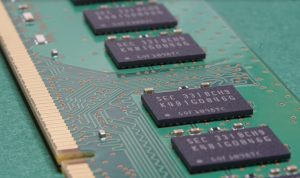
For a product to be robust and generate effective results, it needs to have the right base. A good product is possible only if the manufacturing process is error-free. For something as important as a printed circuit board, it is imperative to choose a company that offers high-quality PCB Board Fabrication process.

A well-rehearsed and error-free manufacturing process will ensure that the printed circuit boards have minimal or zero errors. The holes will be properly drilled, the base would be of good material and soldering would be of the highest quality as well.

In addition, the manufacturer would use the latest techniques and equipment to produce robust and effective printed circuit boards. Only a good circuit board will boost the performance of the electronics. It will also increase its self-life, thus enhancing the brand image of the electronics company.


Read more about: Best PCB assembly manufacturer – Few Tips


General Tips on PCB Fabrication


Nodes accessibility


There is a high probability that you might have to resolve an issue in your Printed Circuit board. In order to do so, you would have to measure signals inside the PCB. For signal measurement, you will need access to the nodes. After all, circuit troubleshooting takes place via these nodes.

Make sure that all the important nodes of your printed circuit board are accessible. If you are hiring a third party PCB Board Fabrication company, ensure that they provide the facility of easily accessing the nodes required for troubleshooting. In addition, the manufacturer needs to test the nodes before rolling out the final product.

A manufacturer can use several ways to test, however, the most popular one is the forming loops that are excellent for testing probes with hooks.


Use same orientation throughout the PCB


The same orientation decreases soldering mistakes as well as makes component inspection easy. Therefore, it is good practice to place components with the same orientation. For example, a standard component pin numbering starts with pin#1 in the upper left corner. Just ensure that all the components pin placement is the same.


The right spacing


Once you have incorporated the node’s accessibility into the design, the next thing that you need to focus on is the right spacing of the components. To ensure the longevity and robustness of a Printed Circuit board, it is imperative for the manufacturer to use the right spacing.

You might be tempted to pack all the components close to each other as this will not only decrease the size of the Printed Circuit board, but it will also reduce the weight. Nonetheless, you need to realize that it is important to leave space for the routing of wires. Ensure that there is enough space for the wire to move between the components.

The amount of space is greatly dependent on the number of component pins. In addition to making the wiring easy, the right spacing will make soldering easier and it will facilitate auto-routing as well.


Exchanging wiring directions Between Layers


On a circuit board, we often see wires crossing each other. Of course, experience ensures that the wires generate the desired results.  To ensure the effective performance of the wires, you need to exchange wiring directions between layers.

A good practice is to have vertical traces on one side and horizontal traces on the other side. In case, you have multiple layers, you should go with alternating between directions.


Match the component sizes


To eradicate component size errors, and to ensure that there is no error in the datasheet, you need to ensure that the components’ sizes match. Instead of finding out later that the components are of different sizes, you should print the layout.

A printed layout will help you resolve if any problem might occur in the future. Take the printed layout and place every component on its respective place on the layout. You now will have a clear idea about component sizes.


Width of Line Selection


A good printed circuit board is also a good heat dissipation. However, not all circuit boards have this capability, therefore you need to ensure that your PCB Board Fabrication manufacturer is experienced enough to choose width of the lines according to the current.

If you go for a larger width, it will reduce resistance and in return, the head due to dissipation is reduced. You need to first estimate the current that will be flowing through these lines and then decide on the width size.

There are several online calculators that will help you decide the width size. So, you really don’t have to put in a lot of effort. Just ensure that the power lines are wider as major current flows through these wires.


90-degree angles with traces


As we mentioned above, having a constant width of wiring is important, but with sharp right angles, this can be extremely difficult. 90-degree angles with traces can be of concern especially when the difference is narrow.

A good PCB manufacturer understands that problem and thus, they will prefer using a 45-degree bend instead of 90 degrees.


Layout vs. Schematic comparison


An experienced Printed Circuit Board would ensure that there is matching between the schematic and the layout of the board. In order to do so, they use high-end and effective software. These software will generate effective results.


 Consider Spots of heat


The heat has an adverse effect on the circuits. If you do not dissipate the heat, your circuit performance will decrease drastically. Excessive heat might also damage the circuit board permanently. Therefore, heat management is important.

You need to consider the component that consumes more power and how to dissipate their heat. A parameter called “Thermal Resistance” monitors temperature increase per watt of power under different situations.

For example, there is a copper area with x by y mm underneath the IC. You will need to incorporate heat sinks or even fan in order to dissipate heat to bring down the IC temperature. You should also isolate the critical parts of the board from the heat sources.


An effective Ground Plane is important


An effective printed board has everything with the same orientation and spacing. So, this means that the voltage should also remain the same in the Printed Circuit Board. This is extremely important, especially in the analog circuits.

There will be a voltage drop in case you trying to use traces to route the ground signal. The resistances created by the routes will lead to the voltage drop. The voltage drop tends to make different grounds in the Printed Circuit Board.

To avoid this, a good idea is to create a ground panel. You can either have a large area of copper or you can reserve a layer of the printed circuit board for the panel. A layer would ensure that components connect directly to the ground through vias.

If you have a complete copper panel, it will dissipate the heat quickly. However, there can be an adverse effect i.e. soldering the panels would be difficult. Nonetheless, it is possible to avoid this by making thin traces.


Keep Analog and Digital Grounds Separate


To ensure that there is no noise, it is a good idea to keep the digital and analog grounds separate.  Current and voltage spiking from the digital circuits leads to the generation of noises in the analog circuits, thus having an adverse effect on its performance.

You can avoid all this by having separate grounds, but then you might have to tie them at some point. So, we suggest you put them together at the end of the supply path. This will serve your purpose as well as avoid interferences. There are other techniques available; however, manufacturer has generally preferred this particular one.


Place Bypass Capacitors


Incorporating bypass capacitors offer a number of benefits. These capacitors have the ability to filter the AC components of the power supply. In addition, there is a reduction in unwanted AC signals such as ripples, noise, etc.

The reduction takes place because the AC fluctuations are bypassed to the ground. So, whatever voltage you want to filter, simply connect the capacitor between it and the ground. For starters, you should go with the Powe inlet of your Printed Circuit Boards as a place for the capacitors.

The wires connected to the power supply often connect a lot of RF signals and they are long as well. If you want other places to place the capacitors, we would recommend incorporating them close to the ICs. Placing the capacitors close to the ground and power pins will reduce the noise present inside the Printed Circuit Board.

The AC components frequencies have a direct impact on the values of the capacitors. Since every capacitor has its own resistance and Equivalent Series Inductance, thus it has its own response to the frequencies. The ESL is tuned to a wide range of frequencies.

For instance, you will need a large capacitors in order to filter low frequencies. Likewise, for mid-range frequencies, you will need a capacitor of 0.1-1 µF. You can go with 1-10µF for low fluctuations and for high frequency, a good idea is to use 0.001-0.1µF capacitors.

Of course, one capacitor is not fit for removing different frequencies. So, a good idea is to use a combination of bypass capacitors. Use 10 µF – 100 µF capacitors for buffering for chips that drive a large volume of current.Manufacturers also use ceramic capacitors mainly because of their size and price. However, not all app capacitor values allow the usage of monolithic ceramic capacitors.


Silk Layer


MCPCB manufacturer uses standard practice of silk layering. The practice makes it extremely useful for labeling. With labeling, you will not only label your components, but it is possible to add information such as the author or the revision number of the circuit board.


Manufacturer specification

\

You will come across several manufacturers; however, every manufacturer comes with its limitation and specification. Some of these specifications include the component spacing, minimum trace width, number of layers, minimum weight and much more.

Before you start on your design, it is imperative to find a manufacturer that can meet with all your Printed Circuit Board needs. Do mention your requirements regarding the material’s grade of the Printed Circuit Board.

The grades range from FR-1 to FR-5. At KingPCB, they generally use FR-4; however, in the case of high-volume consumer applications they recommend FR-2. Nonetheless, the decision of using the grade type mainly depends on the client. After all the type of grade material will have a direct effect on the circuit board’s strength, moisture absorption, durability, and Flame Resistance.


Summary


An experienced PCB Board Fabrication company would understand that a well-designed PCB is perhaps the best. They would know that to deliver quality, they need to have quality at the base. The production system of the Printed Circuit Board should meet the highest possible standards. Of course, with so many PCB manufacturers out there, you will have to choose wisely.

Every company does claim to be the leading MCPCB manufacturer or SMT PCB assembly firm, but they will not deliver what they promise. On the contrary, KingPCB delivers high quality printed circuit board.

They use modern techniques to develop sophisticated Printed Circuit Boards. Their circuit boards are robust and they add value to consumer electronics. They incorporate the right layering technique, dedicate a special layer or large copper area to avoid multiple grounds and incorporate capacitors to dissipate heat.

They will also test the nodes and the spacing of the wires to ensure Printed Circuit Boards run effortlessly in the future. After all, the objective is to deliver high-quality PCBs to the clients within their budget and time-frame.