Categories
PCB Blog

PCB Basic Knowledge: PCB Core Materials and Prepreg Materials

We often refer to the PCB (printed circuit board) plays an important role in the electronics industry. PCBs build a bridge to the world of electronics, so to speak, and the core material and prepreg of PCBs assist in the construction of printed circuit boards.

In this article will take you to understand what is PCB core and Prepreg material, and the differences between them and the application.

What is Prepreg material?

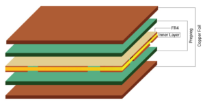
Simply put, Prepreg is a glass fiber with a resin binder impregnation. It is a dielectric material used to provide proper insulation between copper and PCB Core.

Prepreg is also commonly refers to as a bonding material that either combines two cores or a core and a copper foil. This plays a crucial role in PCB design and manufacturing.

The different types of prepreg depend on their thickness and the amount of resin they hold, the higher the resin they contain, the higher the price.

  • Standard resin (SR)
  • Medium resin (MR)
  • High resin (HR)

The process of manufacturing Prepreg
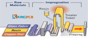
Why is Prepreg so important in the PCB manufacturing process?

  • Easy to apply
  • Facilitates waste management in the manufacturing process
  • Multiple Prepreg options available to meet different needs
  • Helps reduce the weight of equipment

What is a PCB core material?

A PCB core consists of a FR4 (flame retardant) rated glass fiber epoxy laminate with copper laminated on both sides. It is a rigid base material with copper laminated to the instrumentation used to manufacture single-sided, double-sided and multilayer circuit boards.

The difference between PCB core material and Prepreg material

Simply put, core material is the product of prepreg and lamination. As such, it is much more rigid compared to prepreg. Prepreg is partially dry without lamination and is not as rigid as core. The core consists of a glass fiber epoxy laminate which is flame retardant and has copper on both sides.

Another important difference between PCB prepreg and core is its dielectric constant. While the dielectric constant of the core does not change, the dielectric constant of the prepreg changes before and after lamination. The different dielectric constants are also a function of the following factors.

  • Resin content
  • Resin type
  • Glass braid

Explore KingPCB’s services

PCB cores and Prepreg are both important components of PCBs, and understanding these basics is critical to PCB manufacturing.

With over 10 years of combined experience in PCB manufacturing and assembly services, KingPCB offers advanced assembly technology and advanced PCB solutions. More than just high quality, we also offer the most competitive prices.

Don’t hesitate to contact us now to learn more about our PCB services

Categories
PCB Blog

Why is Screen Printing Important for PCB Manufacturing?

What is screen printing?

The term screen printing comes from the process of using stencils on PCBs, also refers to PCB legends, to mark components and provide valid information.

How to do screen printing

Screen printing is the production of a screen-printing plate using hand engraved lacquer film or photochemical plate making by tensing a silk, synthetic fabric or metal screen onto a screen frame.

Modern screen-printing technology, on the other hand, uses light-sensitive materials to produce screen printing plates by photographic plate making methods.

Where to find screen printing?

Screen printing takes place mainly on top of the solder resist layer of the board and is one of the last steps in the manufacturing process.

Common colors used for screen printing are black, white and yellow, however, you can use other colors if necessary.

Although PCBs may technically function without a legend, the information provided by the silkscreen is essential to the user for final assembly, testing and troubleshooting.

Common information displayed in PCB silkscreens are

  • Reference indicators to mark component types
  • Manufacturer information, serial numbers, etc.
  • Test points to aid testing and troubleshooting
  • Component outline indication
  • Marking of component type
  • Component polarity indicator markings

How screen printing is done

Manual screen printing

This can be done with a line width greater than 7 mil and its alignment tolerance of 5 mil. It is not the most ideal option in terms of accuracy as the output depends on many factors such as the viscosity and age of the ink, room temperature, humidity, stroke pressure etc.

Liquid Photo Imaging or LPI 

Use this method when the line width is greater than 4 mil. This provides a higher level of accuracy than manual screening. However, this has a longer set-up time and is known to use more ink.

Direct legend printing or DLP

This method is the most accurate but is more costly and is not suitable for silver panels. In addition, not all manufacturers have DLP printers.

To sum up

With great silkscreen printing helping to reduce the likelihood of errors, correct placement of components and providing additional information about the board.

Silkscreening helps to ensure that parts are assembled correctly and continue to function when they reach the consumer.

Explore KingPCB’s services

A detailed understanding of silk-screening can also reduce PCB costs, whether you are finalizing PCB details or just starting out.

KingPCB has always been a supplier of affordable, high quality PCBs in high volume, whether your requirements are large or small, contact us today to find out more about our capabilities.


Categories
PCB Blog

What is the Cost of Flying Probe Testing?

Well, to start with, our electronic gadgets are going from sleek to sleeker, therefore, board real estate is a precious commodity.

Flying probes have attracted a lot of attention recently, and not just because of the test points. It is a method used for small batches and prototype boards for several reasons.

Today’s era of increasing board density and complexity presents enough obstacles to programming, but flying probes are easy to program.

However, small production runs or prototypes do not really justify the cost of in-circuit testing in a needle bed, where fixtures are expensive. While both methods can detect defects in quality, admittedly the use of flying probe technology offers a cost-effective solution.

What is flying probe testing?

Flying probe testing is an improvement on traditional in-circuit testers. Where a probe is used instead of a bed of pins, and multiple motor-driven, fast-moving electrical probes are used to make contact with the pins of the device and perform electrical measurements.

They operate without a fixed test point. The probes are electromechanically controlled and move according to specific software commands.

Most importantly, the flying probe test does not require a test fixture and can be run directly on the PCB, saving time in the production of test racks, saving test costs and time and making it suitable for small batch PCB and prototype production.

What does flying probe testing check?

  • Opens
  • Shorts
  • Resistance
  • Capacitance
  • Isolation
  • Component values
  • Component polarity
  • Inductance of individual parts

We can carry out other tests with our probes.

  • Phase difference measurement units
  • High voltage pressure tests
  • Miniature short circuit testing

What are the factors that influence the price of flying probe testing?

Volume

The cost of ICT equipment units is relatively high, making flying probe testing more cost effective for small production runs.

Circuit board location and complexity

When testing complex circuit boards it can be difficult to use a fixed position method, flying probe probes can be moved quickly to test in tight locations.

Time

In rapid prototyping, the use of flying probe testing can be effective in reducing test times

Budget

What are the advantages of flying probe testing?

  • Shorter test development cycles
  • Suitable for small production runs
  • Rapid test prototype assembly
  • Quick changeover flexibility
  • Fast feedback

Consequently, for the best results in high quality flying probe testing, work with an electronics contract manufacturer with a proven history of testing services.

Explore KingPCB’s services

At KingPCB, we are fully equipped to meet your PCB manufacturing requirements. Our team of experts and state-of-the-art equipment ensure that all our PCBs meet industry standards for quality and testing.

If you have any questions, please feel free to contact us or by email: sales@kingpcb.com

Categories
PCB Blog

How Solder Paste Helps PCB SMT Assembly

What is Solder Paste?

Solder paste is a kind of gray paste, a new soldering material applied to PCB SMT assembly, which helps to fix electronic components on PCB boards, making electrical connections and mechanical bonds between PCB pads and surface mount devices.

Solder paste is mainly composed of flux and solder powder (Flux & Solder Powder)

The role of flux

  • Removes oxides from metal surfaces
  • Protects the components to be soldered
  • Holds the device in the proper position

What are the factors that affect the function of the solder paste?

  • Uniformity of solder paste particles
  • Percentage of solder powder in the flux
  • Viscosity of the solder paste
  • Thixotropic index and metal content of the solder paste
  • Reflow process

What are the types of solder paste?

According to the flux type, solder can be divided into rosin-based solder paste, no-clean solder paste, water-soluble flux solder paste.

Solder paste in PCB SMT assembly

Reflow Soldering

For reflow soldering in PCB SMT assembly

Create solder joints

Solder paste as a homogeneous mixture of solder alloy and flux, solder paste helps to create reliable solder joints.

Leaded Components

Solder paste helps increase component density and reduce PCB manufacturing costs when assembled with leaded components

Stencil Printing

It helps in adding components to PCBs in established patterns

Jet Printing

Jet printing solder pastes are made from different formulations and therefore the solder paste has a higher fluidity.

Points to note when using solder paste

Make sure the stencil is accurate

Poorly printed stencils can hinder the application of solder paste.

Make sure the screen printer is programmed correctly

Accurate measurement and calibration of the solder paste screen printing equipment is key.

The right amount of solder paste

Excessive amounts and small amounts can lead to errors.

Correct process

You can choose between metal screen printing and mesh screen printing.

Safe handling

Solder paste contains organic solvents. When handling, try to avoid inhaling the fumes released by the solvents during operation, and avoid contact with skin and mucous membrane tissues for too long.

Explore our PCB assembly services

KingPCB has over 10 years of experience in PCB SMT assembly, and we are fully capable of meeting your PCB manufacturing and assembly needs.

You can send your PCB quotation request by email, and your inquiry will be answered within two hours.

Categories
PCB Blog

Complete Guide on Flex PCB Stiffener

Printed circuit board stiffeners provide important mechanical support for PCBs and are often used for flexible circuit boards.

When flexible circuit board components are placed in curved areas and pressure is applied to the flexible material, stiffeners are required to add mechanical strength.

But we need to understand that the PCB stiffener is not part of the board design. Let’s learn more about the role of stiffener and its use.

Where to use stiffener?

Simply put, when the PCB needs to increase the stiffness of the place will need to use stiffener.

  • Support areas with SMT or PTH components
  • To maintain the proper thickness of the flexible circuit
  • Connector areas
  • Areas to keep the circuit stable
  • When limiting flexible parts to a certain position
  • Increasing the bending radius of the circuit at the intersection of rigid and flexible parts
  • Protects solder joints
  • Comply with ZIF connector specifications

How to choose the right PCB stiffener material?

Flexible PCB currently commonly used stiffener materials are polyimide (PI), FR4 and steel sheet.

  1. Polyimide (PI), composed of PI, cover film and adhesive release paper, but the PI layer is thicker.
  2. FR4, mainly composed of glass fiber cloth and epoxy resin adhesive, the same as the FR4 material used in PCB
  3. Steel sheet. The components are steel, with strong hardness and support strength, requires manual assembly, and the process is more complex assembly costs are higher.

How to use printed circuit board stiffener?

In the case of plated through-hole components, the PCB stiffener is located on the same side of the flexible board as the components. This makes it easier to access the pads on the flex circuit. Stiffeners can also be attached to both sides of the part.

Heat and pressure are used when attaching the stiffener to the circuit. Connecting PCB stiffeners requires the use of pressure-sensitive adhesives, commonly used are

  • Pressure sensitive adhesives
  • Thermal bonding adhesives

The type of adhesive depends on the location and/or construction of the stiffener. For example, if the stiffener does not extend to the circuit outline, in most cases it will require a PSA attachment with additional stiffener outline added to the screen for precise placement.

How to distinguish between rigid-flexible PCBs and rigid PCBs using FR4 stiffener?

  1. A circuit board with stiffener is still essentially a flexible PCB, with FR4 stiffener bonded to it to increase rigidity during assembly
  2. Rigid-flexible circuits are known as hybrid flex circuits that include both rigid and flexible substrates, and by definition, rigid-flexible boards are not flex circuits.
  3. The use of stiffener of the flexible PCB stiffener part is no trace, only to enhance the rigidity of the location, they are only mechanical connection between. While the rigid-flexible PCB are designed traces for electrical connections.

To summarize

Use PCB stiffener to protect the components and connectors of flexible circuit swell, to ensure that the circuit does not bend and protect the integrity of the solder joints.

Explore KingPCB’s services

KingPCB, one of the leading PCB manufacturers in China, has extensive experience in manufacturing and assembling rigid PCBs, flexible PCBs and rigid-flex PCBs.

For more information about our PCB supply capabilities, please feel free to email us at sales@kingpcb.com or contact us now!

Categories
PCB Blog

Manufacturing Process for Rigid-flex PCBs

With flexibility and the ability to assemble in 3D, the demand for rigid-flexible PCBs is on the rise. We can say that the importance of rigid-flexible PCBs in PCB manufacturing can not be overemphasized

What is Rigid-flex PCBs?

Rigid-flex PCBs connect rigid PCB materials to flexible materials.

The result is bending only in certain places, making the board more rigid but still flexible.

If you want signals to be transmitted between the rigid and flexible sections, you will need to design a rigid-flex PCB.

In a rigid-flex design, the flexible part of the board resembles a typical flex circuit. At the same time, the material of the rigid part is similar to that of a standard rigid PCB. Like standard PCBs, these rigid areas are usually made of glass fiber as the base material.

Multilayer rigid-flex PCBs also include prepreg glass fibers as an intermediate substrate layer.

However, not all PCB manufacturers can meet the complex flexible printed circuit board manufacturing process. The following are some of the characteristics of rigid-flexible PCBs.

Features of rigid-flex PCBs

  1. Flexibility
  2. Lightweight
  3. Cost effective
  4. Save design and assembly process time
  5. Low noise and high reliability
  6. Resistant to high and low temperatures and fire
  7. Prevent electrostatic interference

Rigid-flex PCB manufacturing procedures

– Material cutting

– Dry film coating

– Automatic optical inspection

– Browning

– Lamination

– X-Ray Inspection

– Drilling

– Electroplating

– Graphic Conversion

– Etching

– Screen Printing

– Exposure and Development

– Surface Finishing

– Depth Control Milling

– Electrical Testing

– Quality Control

– Packing

Rigid-flex PCB design rules considerations

Rigid-flexible boards are much more complex in design than standard PCB design. In particular, we should pay attention to the special places, including the transition area of rigid-flexible, alignment design, over-hole design, etc. All of these items need to follow the requirements of the corresponding design rules.

Over the hole location.

In the dynamic use of the case, especially when the soft board is often bent. It is necessary to avoid as far as possible the soft board over-hole, which is prone to breakage and damage.

The design of the solder pads and vias.

Solder pads and vias in line with the electrical requirements, win the maximum, the connection between the pad and the conductor using a smooth transition line, avoid right angles. Independent pads should be added disk toe to strengthen the support role.

Alignment design.

In the flex zone (Flex) alignment design requirements are best to go rounded lines, rather than angled lines. The opposite of the hard board (Rigid) area recommendations. This can protect the flexible board part of the line in the bending is not easy to break. 4.

Lay copper design.

For enhancing the flexibility of flexible bending of flexible board, laying copper or flat layer is best to use the mesh structure.

The distance between the drill hole and the copper skin.

For the rigid-flexible combination area, the two most important distances must not be ignored. One is the hole to copper distance (Drill to Copper) described here, following the minimum standard of 10 mil. The other is the previously mentioned hole to the edge of the flexible board distance (Hole to Flex), generally recommended 50mil. 6.

The design of the rigid-flexible area.

The line should be a gentle transition, the direction of the line should be perpendicular to the direction of the bend. Wires should be evenly distributed throughout the bending area.

Applications of rigid-flex PCB

Industrial use: industrial, military, medical

Automotive: automotive components, in-car video systems, audio systems, radar imaging systems, satellite navigation, temperature sensors, etc.

Consumer electronics: folding cell phones, video modules, keypads, RF templates, etc.

Explore KingPCB’s Services

KingPCB’s customer support team can help you find the best material and structure for your flexible or rigid-flex PCB. Visit our contact page to send us a message online.

Categories
PCB Blog

Critical factors Affecting the Cost of PCB Manufacturing

There are many factors that determine the cost of manufacturing during the PCB&PCBA assembly and manufacture. Sometimes there are some forgotten indirect factors which can also add to the cost of PCB assembly, such as the number of components assembled, the placement of components, the cost of test equipment, etc.

To better help you understand some of the issues that may exist during the design phase and aspects of controlling costs, please see the following.

Some of the factors that affect the cost of PCB manufacturing.

  • Technologies used in PCBs

Two common technologies used in the assembly process are SMT and THT, and sometimes some components may require both technologies, adding some cost.

  • PCB assembly process requirements

Some PCB assemblies may require some processes are: wave soldering, hand soldering, x-ray, automatic optical inspection etc.

  • Circuit board layers

Circuit boards are generally single-layer, double-layer, multilayer (greater than 2 layers), usually every two additional layers, the cost is different, the more layers, the higher the manufacturing cost.

  • Surface treatment process

Circuit board commonly used surface treatment process are spray tin (Hot Air Solder Leveling), OSP, full board plating nickel gold, sink gold, sink tin, sink silver, chemical nickel palladium gold, electroplated hard gold, some special applications will have some special PCB surface treatment process.

The cost of different finishes varies considerably.

  • Number of components

The cost usually increases with the number of placements required.

  • PCB component size

Usually the installation of smaller components will increase the assembly cost somewhat.

  • PCB board shape

Often there are multiple designs in the assembled PCB prototyping which increase the length of the board as well as the difficulty and also the cost.

  • Certifications

Depending on your needs, some compliance tests such as RoHS, CE, FCC, etc. may be required to ensure compliance.

  • Rigid or flexible circuit board assemblies

Usually flexible PCBs cost more to assemble than rigid PCBs.

  • Testing

PCBs require a number of tests after manufacture and the method of testing is directly related to the cost.

  • Packaging

Different circuit board types have different packaging methods and the cost of packaging varies for different requirements.

Several important tips you need to know:

To ensure that PCBs are manufactured efficiently and correctly, remember the following tips.

  • Ensure a complete and detailed BOM

The PCB BOM is a list of components required for the PCB. It contains details of each component’s model number, manufacturer information, quantity, notes, etc.

In order to obtain a detailed and quick quotation, please provide your manufacturer with a complete and detailed BOM. For more information see how to optimize the BOM.

  • Double-check the manufacturing documentation

For making sure the board you are building is correct, double check the number of holes and their size, through-hole technology, PCB material, PCB layers, etc.

  • Checking

To ensure that your product is manufactured correctly, a number of tests and checks are important and cannot be omitted. It is also to help optimize your time and cost control.

  • Order values and lead times

The more difficult the product, the higher the order value. Confirm assembly and manufacturing times with your manufacturer in advance. So that you have enough time to control your project costs.

KingPCB’s Services

KingPCB has over 10 years’ experience in circuit board assembly and manufacturing. We provide products that meet quality standards and you can rely on us to achieve your perfect circuit board manufacturing.

We offer high quality, efficient, high speed PCB manufacturing, contact us for a quick quote on your manufacturing project!

Categories
PCB Blog

How to Manage PCB Failures?

When a printed circuit board fails, you may face potentially catastrophic and costly consequences. Understanding and preventing PCB failures can minimize the cost of damage.

What causes a PCB failure?

There are three main causes of PCB failure: PCB design issues, environmental and ageing issues.

If there is a problem with the PCB design, it can lead to a variety of problems in subsequent manufacturing processes. For example.

– Inaccurate placement of components

– Overheating due to close spacing of components

Ambient temperature, dust, humidity, etc. during assembly or use can lead to PCB failure.

PCB ageing is inevitable, as everything has its expiry date.

How to fix PCB defeats?

What do you do when your PCB fails? The best way to find out the cause of a failure is to use a printed circuit board failure analysis. The main tests for these are

– Micro-section analysis

– PCB solderability testing

– PCB contamination testing

– Optical/microscopic scanning electron microscopy

– X-ray inspection

Microsection analysis

Microsection analysis of samples is a destructive test, using abrasive paper (or diamond sandpaper) for grinding and subsequent polishing to produce a clear sample profile, and is a rapid method of sample preparation. The use of microsection analysis helps to detect

– Defective components

– Short or open circuits

– Reflow failure

– raw materials

– Thermomechanical failures, etc.

PCB Solderability Testing

PCB solderability testing is used to assess the solderability of components, PCBs, PADs, solder and fluxes by the wetting balance method.

  • Solder and flux quality
  • Quality control
  • Solderability processes

PCB contamination testing

About 15% of PCBA failures are caused by contamination. Ion contamination can cause a variety of problems leading to PCB damage. Testing bare boards for ionic contamination prior to completion of assembly reduces the risk of defects caused by contaminants.

Optical/Microscopic SEM

This method is mainly used to detect PCB soldering and assembly problems.

X-ray inspection

This technique provides a non-invasive method using film, real time or 3D X-ray systems. It can detect current or potential defects, problems involving internal particles, seal cover voids, substrate integrity, etc.

What are the measures to avoid PCB failures?

Use conformal coating

Conformal coatings are one of the main methods of protecting PCBs from dust, dirt and moisture. These coatings range from acrylics to epoxies and are available in a variety of application methods.

  • Manual brush application
  • Spraying
  • Dipping
  • Selective coating

PCB quality testing

PCB manufacturers use a variety of testing methods to check the quality of PCBs during the manufacturing and assembly process.

In-circuit testing

Powering up the board and activating the individual circuits

Flying probe testing

Suitable for sample orders and small quantities

Automatic optical inspection

Photographs of PCBs are taken and compared with detailed schematics to detect boards with markings that do not match the schematic

Aging test

Detects early faults and determines load capacity

X-ray inspection

Function test

Verifies that the board is powered up. Other functional tests include time domain reflectometry, peel test and float test as well as the solderability test, PCB contamination test and micro-section analysis described earlier.

How do I decide on the right test?

Having understood the causes of PCB failures and how to take precautions, you now know what to do next. If you want to minimize PCB failures, choose to work with a PCB manufacturer with extensive experience.

To find out more about our PCB manufacturing capabilities, send us a message now!

Categories
PCB Blog

How Does PCBs Empower the Green Energy Industry

Printed circuit boards play a vital role in many industries.

With the rapid growth of the energy industry and the development of more complex machines, it is essential that these machines and equipment are supported by high quality PCBs and that everything runs as expected.

The Considerations for Renewable Energy PCBs Design

For those interested in renewable energy PCBs, you may want to learn about some of the top design considerations used to create effective PCBs. 

  • Reliability

Since renewable energy PCBs play an important role in providing clean energy in people’s homes and devices. When designing a PCB, you should make sure it will provide reliable performance over time.

  • Size

PCBs for renewable energy applications need to have the right size. For example, solar PCBs are usually small and batteries need to be installed when the sun cannot supply energy to the solar panel. Thus a compact PCB can provide more space for other electronic components.

  • Lead-free materials

Green has now gradually become the world’s mainstream requirements, many PCBs are now using lead-free components and solder to reduce the impact on the environment.

The Challenges of Designing PCBs for the Renewable Energy Industry

When you design a PCB, there are a number of challenges. These include choosing the right materials, ensuring that your PCB has adequate thermal management, and selecting materials with proper signal integrity. Learn more about these key challenges below

  • Power Management

Renewable energy PCBs must properly distribute high power loads to different receivers

  • Signal Integrity

When the PCB is in a high noise and high-power environment, it may be difficult to maintain its signal integrity. Since the renewable energy industry typically requires PCBs to operate in these environments, they must be designed to maintain signal integrity.

  • Materials

PCBs also require that you have materials that work seamlessly in their intended operating environment. In addition to choosing the right materials, you need to make sure that any electronic components you choose are compatible with high-power circuits.

PCBs in the Renewable Energy Industry

The renewable energy industry relies on machines with complex electronics to generate electricity. PCBs help these machines perform at their best, managing their processes and loads while efficiently spreading power across multiple devices.

As renewable energy is the future of energy production, solar, hydropower, wind and geothermal machinery must use PCBs that can meet new demands and help these machines provide reliable power.

  • Hydropower

Hydropower PCBs regularly assist the renewable energy industry. Miniature hydropower systems are entering the consumer market, and anyone with a creek or stream can use these systems to generate electricity. PCBs play a role in many hydropower components, helping hydropower systems to provide you with as much energy as possible

  • Solar

As more and more people switch to solar power in their homes, the demand for solar PCBs is increasing. Solar panel array manufacturers often use high-power and heavy-copper PCBs for their panels, because these boards can better manage the load and keep the panels safe.

  • Wind Power

Companies in the wind energy sector use heavy copper PCBs to assist in energy generation and storage.

  • Geothermal

Geothermal power PCBs must withstand high temperatures and other environmental stresses. Therefore, companies are often equipped with metal core boards for geothermal machines.

These PCBs are good at dissipating heat and are very durable, making them a popular choice for geothermal applications. Geothermal energy is used as a heater for heat pumps in the winter and as a cooler in the summer.

Explore KingPCB’s PCB services

KingPCB is a leading PCB manufacturer in China with over 10 years of manufacturing and assembly experience and is committed to using green materials to manufacture PCBs.

To find out more about our services, contact us now or call us at +86-755 2734 9019

Categories
PCB Blog

Top Guidelines for RF and Microwave PCB Assembly

Radio frequency (RF) and microwave printed circuit boards (PCBs) have the ability to handle higher frequencies than other boards. RF and microwave PCB assembly is also considered to be one of the most reliable designs. As the advancement of technology, RF and microwave circuit boards are used in more and more scenarios.

These PCBs used to be expensive and are most commonly used in aerospace and military industrial applications.

Describe RF and microwave circuit boards

Printed circuit boards combine the complex technology of mixed and digital signal solutions. As the frequency of mixing increases, PCB design becomes more complex. We can think of RF and microwave boards as PCBs that operate at high frequencies. They typically contain components that transmit RF or microwave signals and are capable of handling signals from MHz to GHz frequencies, and are therefore capable of capturing moderate to excessive frequencies. Among the frequencies of the signals, we mention are:

Low frequency signals

50MHz

RF signals

50MHz~1GHz for AM/FM transmission

Mircowave signals

1GHz~30GHz for high bandwidth signal transmission

The normal frequency range for RF is between 500 MHz and 2 GHz, however most board designs above 100 MHz are RF PCBs. any frequency above 2 GHz is a microwave frequency.

RF and microwave PCBs

It was different from each other and are a standard circuit. RF PCBs operate with a high frequency analog signal that can be anywhere between the minimum and maximum limits. Both RF and microwave PCBs operate at a frequency by passing a signal within a specific band. Pass filters transmit signals within the band of interest while filtering out any signals outside the frequency range.

RF / Microwave PCB Assembly Design Guide

If someone needs a guide to assembling RF and microwave PCBs, they should know the basics of microwave PCBs and RF PCBs are necessary. The assembly of RF and microwave PCBs requires specific materials, parts, and techniques. The materials you assemble in such PCBs also need to be of high quality. Make sure you follow the guidelines and consider the following issues:

  1. Highly noise sensitive
  2. Component impedance matching
  3. Return loss
  4. Prevention of crosstalk

RF / microwave PCB assembly in the substrate material requirements

Selecting the best substrate material can result in reliable PCB performance, so it plays a critical role in circuit board design. In the selection of substrate materials, please consider the following matters.

  1. Ensure that the substrate material for RF and microwave PCBs should have a high relative dielectric constant
  2. Consider the temperature stability of the environment
  3. Thicker substrate materials
  4. Relative permittivity and loss angle tangent has a function of dielectric loss

Challenges for RF and microwave PCBs

Design difficulties

In the case of multilayer PCBs, it is necessary to separate different components, such as RF or digital parts and low-level analog.

Noise

RF and microwave signals are more sensitive to noise and are more susceptible to noise compared to standard PCBs. Different types of noise can include white noise, pink noise or band-limited noise, as well as thermal noise, scattered particle noise, phase noise, flicker noise and avalanche noise.

Temperature control

Fluctuations in temperature levels is another issue to consider, temperature changes can affect the material properties of the printed circuit board.

Reliability

When working at extreme temperatures, the reliability of the plated through holes (PTH) used for interconnecting layers is an issue.

Explore KingPCB’s services

KingPCB’s experts can help you with RF PCB fabrication and assembly services that meet your application requirements and budget, while maintaining top quality control and tight lead times.

One of our primary focuses is on high-frequency PCB laminates, so you can trust our expertise in mechanical, electrical, and thermal PCB characterization.

Want get a quote on your PCB project? Contact us now to get more information!


Categories
PCB Blog

How to calculate the cost of a PCB prototype

Introduction

Prototyping occurs at the earliest stages of design and the ultimate goal of prototyping is to obtain an accurate, efficient and successful product that meets specifications.

If you have a PCB project and are looking for a circuit board prototyping service, you may have some questions.

“How soon can a prototype take”

“Do I need a prototype”

“How much does a PCB prototype cost? ” Or other questions.

This article will answer each of these questions.

What is included in the cost of a PCB prototype?

With regard to PCB prototypes, there are several important factors that determine the total cost

  • Board size: relatively speaking, the larger the board size, the higher the cost
  • Materials: Some substrates and PCB lamination materials will cost more. If you need to manufacture high performance multilayer PCBs or HDI PCBs, then the materials will be more expensive.
  • Complexity: If there are a large number of components involved, the total cost will also be much higher for complex and dense wiring designs.
  • Lead time: If your PCB project is urgent, lead time is also in the cost range.

What is the cost range for a PCB prototype?

The cost of a PCB prototype depends heavily on the above factors: size, design, materials, PCB complexity, etc. It is difficult to give an absolute price. Before working with your PCB supplier, you should carefully understand each factor that may add to the cost.

But you can remember the rule of thumb: the smaller the production batch, the higher the cost of prototyping!

The cost difference between producing 1,000 PCBs and producing 10 PCBs is also relatively large, and for 10 boards the assembly costs will be a little higher.

How much time does it take to make a PCB prototype?

As with the cost of a PCB prototype, the time taken to manufacture a PCB prototype is also dependent on the design of the board. The complexity of the board, simple boards can be delivered in a few weeks, while other complex boards can take several months. Of course, there can also be delays in delivery if the supplier is disrupted.

Why PCB prototyping?

Gather more accurate requirements

Developing a PCB prototype can help to consolidate the functionality of the final design requirements.

Understand the problem from a technical point of view

Solve technical challenges that may be encountered in device design.

Identify problems and at low cost

True innovation always involves the risk of failure. By building prototypes, you can quickly weed out ineffective approaches and focus on the ones that work.

Assemble financial support

By developing a prototype to make an idea feasible, you reduce the risk of investment and thus increase the likelihood of securing funding.

Easier patenting

Key components of a patent application, such as patent drawings and inventor’s logs, can be developed through the prototyping process.

To summarise

PCB prototyping is still proving to be the best and safest way to ‘reduce practice’. Sometimes the simplest boards can cause the most trouble, so it is always worth investing in a prototype.

Determining the final manufacturing cost of a PCB prototype requires a lot of work and KingPCB, as a leading PCB manufacturer, can provide in-depth and comprehensive costing to make your design goals a breeze

To find out more about our PCB prototype manufacturing, contact us now or by sales@kingpcb.com.

Categories
PCB Blog

7 PCB Soldering Defects You Should Pay Attention

By understanding the most common PCB soldering defects, you can avoid these defects and protect yourself from PCB failures. Use a list of the most common types of PCB soldering defects to reduce delivery and cost issues associated with bad batches.

Common PCB soldering defects

Even the machine is not 100% correct and everything from operators to contaminants can cause PCB soldering defects.

  • Open
  • Too much solder
  • Component shift
  • Cold joint
  • Soldering bridge
  • Webbing and splashes
  • Lifted PADs

Open

An open circuit occurs when the trace is broken or when the solder is only on the pad and not on the component lead. In this case, there is no adhesion or connection between the component and the PCB. Just like short circuits, these can also occur during production or soldering and other operations.

Too much solder

When too much solder is used, large solder bubbles form in the joints. The joint itself works fine, but hides trouble under the PCB solder ball.

Component shift

Component shifts occur when the PCB is not aligned on the target area. Improper design of PCB parts direction will also cause short circuit of the board. The way to reduce this is to make sure the PCB is centered and has a horizontal surface or a correct reflux curve.

Cold joint

When the temperature of the iron is not heated enough, or at low temperature, cold joints will occur, which may limit the function of the PCB.

Soldering bridge

When two points on a circuit board that were not designed to be electrically connected are inadvertently connected by solder through the top of the PCB solder mask, this creates an electrical short circuit that can cause a variety of damage. Generally welded Bridges are difficult to notice and often go undetected.

Webbing and splashes

When soldering is affected by contaminants, webbing and spatter will appear, affecting the appearance of the PCB and even causing a short circuit.

Lifted PADs

When not enough solder is used on the pads, they are rough or overheated and they are subjected to excessive force, THE PADS MAY be ELEVATED from the PCB and a short circuit may occur, damaging the entire board.

Want to know more about PCB defects?

Working with a qualified PCB manufacturer can help you complete your PCB project without worrying about PCB defects.

To ensure that your PCB is first class, KingPCB provides reliable measures and services in the production process. Contact us now for any more information about PCBs.