Categories
PCB Blog

Why is PCBA First Article Inspection Important?

What is First Article Inspection?

First Article Inspection (FAI) is one of the important processes before massive PCBA manufacturing. The production line processing a certain number of products, after a full range of testing, can reduce the risk of errors in the production process, and improve production quality.

Through FAI, can find many problems such as fixture wear or installation positioning errors, measuring instrument accuracy problems, material feeding, recipe errors, and other causes, so corrective or corrective measures can be taken.

What circumstances require the FAI?

  1. When a new product is launched for the first time
  2. At the beginning of each work shift or handover
  3. Product type
  4. Adjustment of equipment, fixtures, loading
  5. Technology, process, and parameters changing
  6. New material
  7. Change of laboratory fluid, etc.

What is the standard of the FAI?

Three-inspection system:

  • self-inspection
  • mutual inspection
  • transfer inspection

The products sent for inspection need to be checked by the operator for the first time, then by the production team leader, and finally by the inspector to check and confirm that they are qualified before processing.

The inspector needs to do the required markings on the inspection of qualified products (such as the endorsement “first qualified”, etc.). Maintain until the class or a batch of products is processed (all the first products must be left as a sample for subsequent product comparison, to see whether the process changes and mark with a marker “√ ” to show that through the FAI)

The FAI should be done in a timely manner when the first record, fills out the FAI confirmation.

What are the major items of the FAI?

  1. The drawing number is consistent with the work order
  2. Consistency of materials, embryos or semi-finished products in the work order
  3. The surface treatment and installation positioning of the material and embryo are consistent
  4. Whether the material is in accordance with the requirements
  5. Quality characteristics of the first parts are in accordance with the requirements specified in the drawings or technical documents

Attention of PCBA FAI process

  1. Protective measures, such as electrostatic protection
  2. Position, polarity, angle, etc. of the mounted components meet the requirements of technical documents.
  3. Is the quality of the incoming material of the components qualified, such as component color, component size, positive and negative polarity, etc.
  4. Is the welding quality of the components meets the requirements of the relevant technical documents.
  5. The inspector should make a mark on the first piece of qualified inspection according to the regulations, and retain it until the completion of the batch of products.
  6. The first inspection must be timely, so as not to reduce production efficiency.
  7. The first piece without passing the inspection, shall not continue processing or operations.

In short, the above is the PCBA processing process may encounter problems and preventive measures, we hope it will be helpful to you

KingPCB’s service

KingPCB provides a one-stop PCBA manufacturing platform, accepting samples/small orders, SMT placement, PCB prototyping, PCB assembly, and electronic component procurement services.

Contact us today to get more information.

Categories
PCB Blog

How to Protect ESD During PCBA Processing?

Introduction

PCBA refers to Printed Circuit Board Assembly, meaning the process of placing components on the board through SMT or THT PCB assembly

PCBA board has many precisions electronic components, which are sensitive to voltage. Higher than the rated voltage shock will damage these components, resulting in functional testing of the PCBA when it is difficult to check, leading to defects when delivered to customers, bringing a lot of rework pressure.

So in the PCBA fabrication process of electrostatic protection is crucial. Doing a good job of electrostatic protection can effectively protect the electronic components.

What is Electrostatic Discharge?

ESD, Electrostatic Discharge is an electrical charge at rest. Human electrostatic momentary current can reach more than 10,000 volts, and rubber, plastic film surface electrostatic is up to 100,000 volts.

The basic physical properties of static electricity are: attraction or repulsion, and the earth has a potential difference, will produce a discharge current.

These three characteristics can be three effects on electronic components are

  • Dust, reducing the insulation resistance of components (shorten the life).
  • Damage, resulting in electronic components cannot work.
  • Amplitude of the electromagnetic field is very large (up to several hundred volts / m) extremely wide spectrum (from tens of megawatts to several gigawatts), causing interference and even damage to electronic products (electromagnetic interference)

What are the effective electrostatic protection measures?

(1) Operators should wear anti-static wristbands when operating.

(2) The human body through anti-static shoes (or shoelaces) and anti-static floor grounding, it should comply with the relevant provisions of GB4385-1995; general circumstances allow the wearing of ordinary shoes, but should be used at the same time conductive shoe bundle or heel strap.

(3) Anti-static work clothes, it should comply with the provisions of GB12014-2009. In an environment where the relative humidity is greater than 50%, they are allowed to choose pure cotton products.

(3) Work surface grounding.

(4) Test instruments, tool clamps, soldering iron grounding.

(5) Anti-static floor, ground (table) mat, trolley, box, frame, and chair

Attention:

  • All components must be operated on the anti-static safety workbench.
  • If the operation inadvertently electrostatic sensitive components dropped on the ground, must be tested before use
  • When holding sensitive components by hand, direct contact with their leads and lug should be avoided. When taking the motherboard should avoid contact with the sensitive component area.

To sum up

In short, all objects in contact with the board or components, should have anti-static measures.

KingPCB as one of the leading PCB manufacturer, provide various anti-static operating system to provide best quality to our customers.

Contact us today to get more information about our measures!

Categories
PCB Blog

How to Avoid PCB Tombstoning Defects?

A tombstone defect is a kind of PCB failture. Tombstoning defects occur frequently and are caused by surface mount passive components that are partially lifted from the pads and erected to look like tombstones. But it is not as deadly as a burned component and can be 100% avoided.

What is a tombstone defect in PCB?

Tombstone defects are also called Manhattan effect, Stonehenge effect, or drawbridge effect. It occurs due to torque imbalance caused by different wetting humidity. Wetting is when the solder reaches a fluid state in order to attach the component leads to the pads. Ideally, the solder adheres to both pads while the wetting process is uniform, but unbalanced soldering can result in a standing monument.

Tombstone printed circuit boards are not limited to passive devices; it can also occur on SMT devices.

What are the causes of PCB tombstone defects?

– Unsuitable solder pad design

– Incorrect component placement

– Inconsistent pad size

– Nitrogen

– Uneven reflow oven temperature

– Chip placement parallel to reflow oven

– Inconsistent heating capacity of PCB material

How to avoid tombstone defects in PCBs?

Like other common PCB soldering defects, tombstone defects can be prevented. Please consider the following points.

PCB pad size

Always need to check the pad size is correct, too big or too small can lead to tombstone defects.

PCB surface treatment process

For small size components such as 0201 or 0402, avoid using traditional hot air solder leveling (HASL), which can lead to uneven surfaces.

PCB component placement

In the case of small components encountered, ensure that the alignment widths of the connection pads are equal and they should also be connected in a similar orientation.

Solder resist layer thickness

Ensure that the thickness of the solder resist layer is appropriate to prevent oxidation while not restricting the movement of the solder.

Inner copper overlay

Uneven copper coverage can lead to uneven heating.

Stencil design

A proper stencil design should ensure that there is sufficient solder paste, and in addition, there should be proper component overlap with the paste.

PCB testing

Each component needs to be tested to avoid affecting the function of the PCB. Common PCB tests are

-In-line testing

Flying probe test

Automatic optical inspection

-Aging test

-Other functional tests

Trace wiring and power supply layer

The balance of PCB wiring is crucial.

To summarize

PCB soldering defects can lead to PCB failures, resulting in costly recalls and rework. To avoid possible PCB defects, it is important to choose an experienced PCB contract manufacturer. kingPCB provides one-stop PCB manufacturing services with professional wisdom, reliability testing and versatility.

If you have any questions, contact us now or by sales@kingpcb.com and we will respond immediately to any of your requests!

Categories
PCB Blog

Six Reasons for PCB Failures

Just like the age of people, everything has its shelf life. PCB is the lifeblood of the electronic equipment we use, many devices rely on the circuit board, so we must pay attention to the board failure. PCB failure and many reasons, from production in the hands of the final customer use, any one of the links can go wrong. Through this article to understand the common causes of PCB failure, you can easily prevent possible future PCB failure problems.

PCB failure common 6 reasons

  1. PCB defects

Defects are the most common cause of PCB failure, usually generated during the PCB assembly process. Circuit boards are very sensitive to electrostatic discharge (ESD), static electricity generated by thousands of volts can easily damage the PCB components. Other potential defects are unaligned layers, short circuits, cross signals, etc. Reliable PCB manufacturers back to take a variety of preventive measures to eliminate electrostatic discharge on the production floor.

  1. Component problems

Component burn-in is a PCB defect, notably it is the main cause of PCB failure. This requires not only the replacement of parts, there is the possibility of repairing the entire board. Causes of component burn-in include extreme heat, components spaced too close together, the board is not properly connected, etc.

  1. Environment

Circuit boards are also sensitive to external factors. For example, hair, dust, liquids, fibers and other foreign objects in contact with the board can have an adverse effect on the product. In addition, excessive heat and humidity may cause the PCB to expand and thus warp and damage the solder joints.

  1. Solder problems

Solder connects components and circuit boards and is a key component in the PCB process. If the solder is contaminated, or contains too much moisture, it may cause the board to short circuit. There are several common solder defects.

-Open

-Excessive solder

-Component displacement

-Solder bridges

  1. Human error

During the production process, there may be some human errors that lead to PCB failures.

-Misreading the schematic

-Miss installation of components

-Bad soldering

  1. Equipment aging

Every device has its life cycle, after reaching the life cycle may begin to fail, it is a wise move to replace the PCB with a new one, or use a small part of the new one to repair the board.

 How to fix PCB failures?

Ultimately, replacing components and redesigning products is part of the PCB business. Having a partner that understands the details of PCB testing, assembly and remanufacturing can save you time and money.

Choose KingPCB as your PCB supplier, we have a professional team to assist you to better complete your PCB project, contact us now for more information about quotes!

Categories
PCB Blog

Multi-layer PCBs Advantages and Applications

As society’s technology evolves and PCBs power many industries and devices, our demand for different types of PCBs continues to grow.

Before investing in a new PCB, you should understand the advantages and disadvantages of each option. As far as wiring is concerned, the more layers the better for wiring, but the cost and difficulty of making the board also increases. So, the choice of layers needs to consider all aspects of the needs to achieve the best balance.

What is a multilayer PCB?

Single-layer PCBs are usually used for simple devices with only one layer of conductive material, and you will find the conductive wiring pattern mounted on one side of the board and the components mounted on the other. Double-layer PCBs are similar to single-layer PCBs but have more functional layers than single-layer PCBs, and double-layer PCBs have two conductive layers.

Multilayer boards are more complex than double-layer boards, with three or more layers of conductive materials, two of which are on the outer surface, while the remaining layer is synthesized within the insulating board. The electrical connection between them is usually achieved through plated through-vias in the cross-section of the board.

Advantages of multilayer PCBs

Circuit boards determine the process difficulty and processing price according to the number of wiring surfaces. For high-end electronic products, in addition to surface wiring, multiple layers of circuits can be stacked inside due to the product space design factor. In general, these boards are smaller and lighter, ideal for smart products, the following are the specific advantages of multilayer PCBs.

  • Multi-layer circuits offer more functionality
  • Provides faster speeds than single-layer PCBs, double-layer PCBs
  • Longer life of the board
  • Has rigorous testing during the manufacturing phase
  • Applicable to both rigid and flexible structures

Limitations of multilayer printed circuit boards

Despite the many advantages of multilayer printed circuit boards, there are some disadvantages that cannot be ignored

  • Increases manufacturing costs
  • Longer manufacturing time
  • Relatively more difficult to maintain

Applications of multilayer printed circuit boards

Products in many industries can benefit from multilayer printed circuit boards.

  • Computer equipment
  • Medical equipment
  • Fire alarms
  • GPS and satellite systems
  • Industrial control equipment
  • Military applications, etc.

Turn to KingPCB for your projects!

KingPCB is a leading supplier of multilayer printed circuit boards. We provide reliable multilayer printed circuit board products for a variety of industries from medical instrumentation to test services.

Contact KingPCB today to learn more about our PCBs and to select the solution that best fits your needs.

Categories
PCB Blog

All You Need to Know about Laser Drilling

With the recent development of industry and science and technology, for high precision printed circuit boards, conventional drilling technology can no longer meet its needs. Laser drilling provides a new way. It is used to drill PCB micro holes and can ensure the accuracy of the holes.

What is PCB laser drilling?

Laser is a powerful beam of light that is excited when the “rays” are stimulated by an external stimulus and the energy is increased. Laser drilling was the first laser processing technology to reach practical use and is one of the main application areas of laser processing.

It is becoming increasingly important as it is commonly used for HDI printed circuit board microvias. IPC defines microvias with dimensions equal to or less than 0.006 inches (0.15 mm). In this case, mechanical drilling is no longer sufficient, and laser drilling provides good control of accuracy and controlled depth.

Mechanical Drilling V.S. Laser Drilling

Mechanical drilling

-Causes drill vibration

-Unsuitable for holes less than 6 mil in diameter

-Not suitable for precise depth control drilling

-Takes a long time and is expensive

-Requires manual adjustment

Laser drilling

-Vibration-free drilling (non-contact)

-High accuracy

-High aspect ratio

-Multifunctional (laser machines can also perform processes such as welding and cutting)

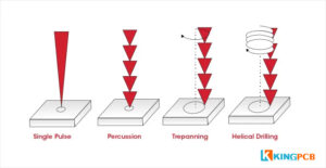
Different types of laser drilling

-Single pulse laser drilling. It is a type of drilling where both the laser source and the working material remain stationary and emit a single laser beam

-Percussion drilling. Sends a series of laser pulses that can create deeper and smaller holes

-Treoanning. The laser beam is guided around a predetermined trajectory.

-Helical drilling. The laser beam follows a spiral path while rotating around its own axis

Two laser technologies are available for laser fine drilling of circuit boards in the drilling process of the PCB manufacturing process.

  1. CO2 laser wavelength in the far infrared wavelength band. (currently more widely used)
  • UV laser wavelength in the ultraviolet wavelength band.

Summary

The best choice of laser drilling for making micro holes, KingPCB, as one of the leading PCB manufacturers in China, has a wealth of experience in PCB manufacturing and assembly, and is committed to providing the best PCB manufacturing services to our customers.

If you have any questions, contact us to get more information!

Categories
PCB Blog

PCB Trace Widths and Precautions

No matter what industry you are in, you probably use products or equipment containing printed circuit boards every day. Regardless of the type of PCB you use, they should be designed with the proper trace width for operation.

PCB Trace Width

Trace widths are measured in mil or thousandths of an inch. Generally speaking, the standard trace width is between 7-12 mil. Typically, 10 mil is chosen for low frequency and small currents, and high-density PCBs may require trace widths as thin as 2.5 million.

PCB trace width determinants

  • The size of the current
  • Working frequency high or low
  • PCB board area and complexity

PCB trace width in the layout of the role

Trace width affects the electrical performance of the PCB, including

Signal Integrity

Using different trace widths can improve signal integrity and control signal interference, crosstalk, etc. When it comes to certain high-speed signals, they need to be routed at a specific width for impedance control. Calculation of the trace width needs to be based on the following factors.

  • Dielectric material
  • Spacing to other signals
  • Copper weight

Power Integrity

To ensure power integrity, here are a few tips to consider.

  • Keep the traces short and direct
  • Use wide traces
  • Consider heat dissipation and current levels

PCB layout considerations

  • The first principle of layout is to ensure the cloth through rate of wiring, pay attention to the connection of flying wires when moving devices, and put devices with connected relationships together.
  • Digital devices and analog devices as far away as possible
  • Decoupling capacitors as close as possible to the device’s VCC
  • Place devices not too dense.
  • More use of Array and Union functions provided by the software to improve the efficiency of the layout.

How to choose the best PCB trace width?

PCB layout engineers can design multiple PCB CAD tools to control the width of the trace by specifying the width and spacing of each network to control the individual networks. Using CAD tools can also set the network category. Some CAD systems also offer the ability to set different rules for specific areas. This can be very useful as you move through dense areas.

Choose a strong PCB contract manufacturer

To ensure proper use of tools to meet the highest quality standards for PCBs. kingPCB takes many effective steps to meet your PCB manufacturing requirements, providing quick turnaround and on-time delivery for your customers.

Provide us with your PCB Gerber files and BOM sheets via email and we’ll get back to you with an answer and quote as soon as possible!

Categories
PCB Blog

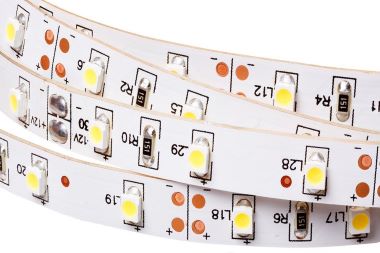
Best Practice Metal Core Printed Circuit Board in LED Products

Printed circuit boards have greatly expanded the development of electronic applications. Metals are good conductors of electricity and transmit power to different components.

Metal core PCBs are often used in the LED lighting industry, power supplies, amplifiers, etc. So, what are LED products?

What are LEDs products?

LEDs are widely used in a variety of lighting products, as well as certain accessories. Compared to other conventional products, LEDs are very cost-effective, but heat loss makes LEDs sometimes unstable and unable to achieve maximum efficiency for use. To solve this problem, metal core PCBs are a good solution.

What is a metal core PCB?

Metal core PCBs are similar to standard PCBs, with the difference that the addition of metal layers to metal core PCBs adds a variety of advantages that have led to their widespread use. Because of their exceptional quality and high thermal conductivity, metal-core PCBs are considered a better choice than glass epoxies.

The most commonly used metal for metal core PCBs is aluminum

Which is an inexpensive metal with good thermal conductivity, and copper is the second most commonly used metal. The choice of aluminum or copper depends on which metal is more suitable for the product you are designing, the main difference between Aluminum and Cu:

-Copper PCBs have better heat transfer and dissipation than aluminum PCBs

-Aluminum is lighter than copper, making it the best choice for lightweight LED PCBs

-Aluminum is cheaper

What is the difference between metal core PCBs and FR4 PCBs?

  • Thickness

FR-4 PCBs have more options when it comes to thickness, but metal core PCBs have limited variation, which depends on the thickness of the backplane and the thickness of the dielectric sheet.

  • Heat dissipation

Metal core PCBs can dissipate heat through holes, whereas FR-4 PCBs transfer heat through holes.

  • Solder

Metal core PCBs have a white resist layer and are only used on the top, whereas FR-4 PCBs have a wide choice of resist layer colors for the top and bottom.

  • Electrical Conductivity

Metal is a conductor of electricity and therefore metal core PCBs have a higher electrical conductivity. The thermal conductivity of metal cores ranges from 1w-4w, whereas FR-4 only offers a thermal conductivity of 0.3w.

  • Plated through holes

PCB plated through holes are not suitable for metal core single layer PCBs, metal cores are more suitable for SMT.

  • Stiffness

Metal core PCBs are able to withstand more tremendous shock and vibration and are 2-4 times stiffer than FR-4 or polyimide.

  • Cost

Metal core PCBs are somewhat more costly than FR-4 PCBs.

What makes metal core PCBs the best choice for making LED products?

Metal core PCBs play a key role in overheating components, transferring heat from one side to the other where it disappears, thus increasing the life of the product. While LED products need to emit a lot of heat, metal core PCBs can quickly transfer heat to prevent overheating. Aluminum is also a more stable metal than other metals, making it more suitable for use in LED products.

The metal core PCB is also highly conductive and has enough space to accommodate LEDs, thus increasing the density of the LEDs and producing enough light for high performance.

At KingPCB

We offer the highest quality metal core PCBs, and with high reliability, fast delivery, competitive pricing and over 10 years of manufacturing experience, you can trust us to meet any of your PCB project manufacturing needs!

To get more information about PCB manufacturing and PCB assembly services, and explore our PCB manufacturing services. Get a quick quote at sales@kingpcb.com or call us at +86-755 2734 9019

Categories
PCB Blog

PCB Temperature Guide

PCB temperature is an important indicator of safety, reliability and performance. Excessive temperatures are likely to cause failures and permanent damage.

During the PCB manufacturing process, there are several conditions that can generate more heat. For example, external component mounting, drilling and soldering processes, inadequate environmental ventilation and other factors can generate excessive heat, which can lead to damage to the board.

In either case, effective PCB cooling techniques and PCB thermal management can significantly control excessive PCB temperatures. In this article we will explain in detail there are issues related to PCB temperature.

How to measure the PCB temperature?

Before measuring the PCB temperature, you first need to determine the main heat source in the PCB, usually a microcontroller or processor, or locate the temperature sensor.

Next, find the connection to the ground (GND) pins of the heat source substrate. most of the heat generated in the PCB is transmitted to the temperature sensor through these pins.

Then we can start measuring the PCB temperature, which usually involves the following three steps.

  1. Place a grounding layer between the temperature sensor and the heat source
  2. Connect the GND pin of each temperature sensing to the ground layer of the heat source
  3. Ensure that the temperature sensor and the heat source on the PCB remain close to each other

Common causes of high PCB temperatures

How much heat a PCB can withstand depends on the materials used to make it up. Materials with the best thermal properties can effectively resist the effects of temperature. In the selection of materials for PCB, you can choose a high TG material.

Some common causes of high PCB temperatures are.

  1. Component failure.
  2. Through-hole interference.
  3. Surface mount component distance.
  4. High frequency circuits. 5.
  5. Lead-free solder.

Why is it important to measure PCB temperature?

It is important to monitor the PCB temperature, too high a temperature can led to structural changes in the performance of the PCB, or even damage.

Overheating in the PCB can lead to damage to the following.

– Structural integrity

– Circuit interruption

– Different material expansion rates

– Oxidation

How to prevent excessive PCB temperature?

To prevent the PCB from heating up, engineers can take the following PCB cooling techniques.

Use heat sink

Heat sink can effectively and safely dissipate heat.

Use a cooling fan

Cooling fan allows the temperature to dissipate while allowing cold air to enter, helping to prevent the PCB from overheating.

Select heat-resistant materials

Compared to standard PCBs, thick copper PCBs have excellent resistance to high temperatures and can handle higher levels of current and provide stronger connection points.

Increase the board thickness and width

In PCBs, thicker boards tend to be less efficient than thinner boards in terms of thermal conductivity, which means that more power is required to enable thicker boards to reach high temperatures, which can effectively avoid PCB overheating.

Application laminate

High-temperature PCB laminates can prevent overheating by providing thermal protection for PCB components.

Use similar coefficient of thermal expansion materials

The coefficient of thermal expansion (CTE) measures how much a material expands when exposed to high temperatures. In a PCB design, the ideal dielectric layer has a similar CTE to the copper layer. this way, if the layers expand, they will expand in a uniform manner, thus minimizing damage.

Maintain adequate spacing

When circuit board components are too close together, it may lead to crosstalk and increased alignment resistance, resulting in resistance loss and increased circuit heat.

Integrate heat pipes

The liquid in the PCB heat pipe piping absorbs heat and prevents it from damaging the board components.

Contact KingPCB

When you are looking for a PCB that can be specifically designed for temperature control, KingPCB is your trusted partner with extensive manufacturing and assembly experience to help you evaluate your project, and a professional team to help you manufacture your PCB efficiently.

Contact us today for a quote or for more information.

Categories
PCB Blog

Best Complete Guide to Vias in PCB Design

With the progressive miniaturization of electronics, surface mount technology has become increasingly popular. Essentially, vias are small vias that pass through a PCB laminate. Vias are essential in multilayer boards because they create connection paths between different layers of the printed circuit board.

What are the types of PCB through-vias?

Depending on the needs of the application, as well as the location of the vias in the stack and the number of layers they pass through, the commonly used vias can be divided into three types.

– Through vias

Through vias indicate that they pass through all layers of the PCB and are open at the top and bottom layers of the board. They usually have a larger size than other types of vias. It was the most common and most commonly used.

– Buried vias

Buried vias, as the name implies, are vias buried in the inner layers of the board, not connected to the outer layers, and are commonly found in multilayer PCBs. It is useful for reducing the PCB aspect ratio (PCB thickness to through-via diameter ratio is also very useful)

– Blind vias

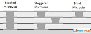
These vias start from the outer layer of the board and go through one or more inner layers, but are not connected to the other side, while through vias connect both sides of the board. Blind vias are useful for increasing the number of connections between the internal and external layers, effectively reducing the number of alignments and increasing the efficiency of the PCB’s use.

Other vias in the PCB

– Vias in pad

Along with the move to higher integration densities for electronic components, this also means an increase in the number of interconnect pins. Designers use vias applied directly to BGA (ball grid array) pads, also known as vias in the pads, in their designs. It reduces the space needed to use the PCB, resulting in a smaller board. However, vias in pad may cause the vias to fill up during the soldering process, making them unusable.

– Laser Microvia

Microvias are the smallest through-vias, typically about 0.003″ – 0.004″ in diameter (equal to or less than 150 µm). It was explicitly used in boards with many interconnects(HDI PCBs). The aspect ratio of micro vias is 1. It requires laser equipment to drill through holes, which is relatively costly.

– Thermal vias

Thermal vias are used to conduct heat to the back side of the PCB by using the perforations of the PCB. Active components, high performance microprocessors and high frequency components generate a lot of heat. In order to dissipate heat effectively, the thermal vias must be placed as close as possible to the component generating the heat.

How do I determine the correct vias for my PCB?

There is a strong relationship between the type of through-hole and the size and function of the board. In larger devices with boards, PCBs with through-vias components may be more efficient. On the other hand, for smaller devices, micro-blind vias work best, but the investment cost may be relatively high.

When you communicate with your manufacturer, you must clearly state your through-hole requirements in the manufacturing documentation, preferably using a separate document stating the through-hole requirements.

To sum up

The popularity of miniaturized and high-density designs for appliances has made through-holes increasingly important, and their role is

– Increase board alignment density

– Aids in signal transmission between different layers

– Helps build component density

Contact Us

KingPCB has over 10 years of experience in PCB manufacturing and assembly in China, not only for conventional circuit board manufacturing, but also for providing high precision multilayer PCB vias.

Our quick response, high quality manufacturing, and timely delivery capabilities set us apart from other manufacturers. If you have any questions or would like a quote for your project, please feel free to contact us via email!

Categories
PCB Blog

Completed PCB Surface Treatment Process Guide

Why is it necessary to process the surface of PCBs?

As copper in nature tends to exist as an oxide in the air, it is unlikely to remain as virgin copper for long and therefore other treatments are required. Oxidized copper can have multiple effects on soldering, such as the formation of fake solder, mis-soldering, or even the inability to solder pads to components. So to prevent this, PCB manufacturers add a special process when manufacturing – the surface of the pad is coated with other substances to protect the pad from oxidation.

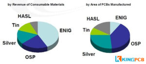
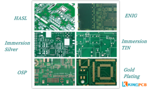
The current mainstream PCB surface treatment process has six types

HASL (Hot Air Solder Leveling)

OSP (Organic Surface Protection)

ENIG (Electroless Nickel/Immersion Gold )

Immersion Silver

Immersion Tin

Gold Plating, etc.

Different surface treatment processes are used in different scenarios, so it is important to choose the most suitable and cost-effective one.

Bare Copper Board

Advantages

Low cost, flat surface, good solderability

Disadvantages

Easy to oxidize, cannot be used on double-sided boards, if there are test points, solder paste must be added to prevent oxidation, otherwise, the subsequent contact with the probe will not be good.

HASL (Hot Air Solder Level)

HASL is a process of coating the PCB surface with molten tin-lead solder and leveling it with heated compressed air to form a coating layer that is resistant to copper oxidation and provides good solderability. The hot air leveling process forms a copper-tin metal compound at the bond between the solder and the copper, which is approximately 1 to 2 mil thick.

Advantages

Lower price, better solderability

Disadvantages

Not suitable for soldering pins with small gaps or components that are too small, and the surface flatness of the solder plate is poor, which can easily cause solder beads in the process and short circuits to fine pitch components.

OSP (Organic Soldering Preservative)

This is a chemically grown layer of organic skin that acts as a barrier between copper, and air. This film is resistant to oxidation, thermal shock and humidity and protects the copper surface from further rusting (oxidation or sulfidation, etc.) in the normal environment; at the same time, it must be easily and quickly removed by the flux in the subsequent high soldering temperatures to facilitate soldering.

Advantages

Simple process, low cost

Disadvantages

Susceptible to acid and humidity, needs to be resurfaced after more than 3 months, OSP is an insulating layer, so test points must be stamped with solder paste to remove the original OSP layer in order to access the pinpoint for electrical testing.

ENIG (Electroless Nickel Immersion Gold)

ENIG is a thick layer of electrically good nickel-gold alloy on a copper surface that protects the PCB for a long time and has good resistance to the environment.

Advantages

Not easily oxidized, flat surface, suitable for soldering fine gap pins and smaller components. First choice for PCBs with keys and can serve as a base material for COB (chip on board) marking.

Disadvantages

Higher cost and poorer solder strength. The nickel layer will oxidize over time and long-term reliability is an issue.

Immersion Silver

Between OSP and chemical nickel/immersion gold plating, is a displacement reaction and it is almost a sub-micron coating of pure silver.

Sometimes the silver immersion process also contains some organic matter, mainly to prevent silver corrosion and to eliminate silver migration problems.

Advantages

Relatively simple process, fast, good flatness and contact.

Disadvantages

Provides good electrical properties and maintains good solderability even when exposed to heat, humidity, and contamination, but loses luster. And because there is no nickel under the silver layer, immersion silver does not have all the good physical strength of chemical nickel/immersion gold plating.

Immersion Tin

The process creates a flat copper-tin intermetallic compound, a property that gives the same good solderability and good flatness as hot air leveling.

Advantages

Compatible with any type of solder.

Disadvantages

It should not keep for too long, and the process of tin dipping contains carcinogenic substances.

Gold Plating

It is mainly plated on nickel plating, as gold and copper, iron between the barrier layer. The main role is to prevent gold and copper, iron between the mutual diffusion.

Advantages

Strong corrosion resistance, good electrical conductivity, easy to weld. High-temperature resistance, with a certain degree of wear resistance

Disadvantages

Relatively high cost, uneven thickness, plated parts require electrical connections.

Categories
PCB Blog

Impact PCB Cost of Different Technical Factors

PCB design and manufacturing involves many different technologies, depending on the different application scenarios of the board. The technology required is also different, such as everyday consumer electronics and industrial-grade PCBs, industrial-grade circuit board manufacturing costs and technical requirements are obviously relatively high.

The main factors affecting the cost of PCB is the material, size, number of layers, surface treatment and vias, of course, there are other factors, depending on the requirements of the PCB design.

Material selection

The cost of different PCB material selection is also different. the most commonly used material for PCB is FR-4, for different application scenarios, the factors affecting the choice of material may be the following.

-Temperature requirements

-Heat transfer

-Signal performance

-Mechanical properties

PCB Size

The size of a PCB will generally be determined by the number of circuits required for the respective device. For small devices such as cell phones, wearable devices, etc. require relatively few components, while the size of the PCB in larger devices will be larger.

Number of layers

Another important factor that affects the price of circuit boards is the number of layers. Obviously, the complexity of production of multilayer circuit boards (greater than two layers) also leads to an increase in its cost. Overall, each additional two layers may lead to an increase in cost of 30% to 40%, although the specific circumstances need to be evaluated.

Surface treatment

PCB production on the need to consider a factor is the surface treatment technology. The most common surface treatment is HASL, which provides good solderability, for higher requirements of the PCB, ENIG will be a good choice, but the cost is also relatively higher.

Vias

The size and number of vias is also one of the important factors affecting the cost of PCB production. More vias means more work. The general size of the via diameter is not less than 0.3mm, less than this value may require the use of light drilling equipment. Different types of vias require different technologies for HDI PCBs involving vias such as blind vias, micro vias and buried vias, which have certain requirements for the PCB manufacturer’s manufacturing capabilities.

Minimum track space

In order to make the effective transmission of current on the PCB, the board must be designed with sufficient alignment width, the alignment width to a certain extent determines the carrying capacity of the board.

PCB thickness and aspect ratio

The standard thickness of the PCB is 1.6mm (0.063 inches). In general, the cost of thicker circuit boards will be more expensive. Thicker boards also have a larger aspect ratio, and it can be significantly more expensive. For your board thickness manufacturing requirements, consult the PCB manufacturer for more information.
Other custom requirements

Unique circuit board designs often require additional processes, such as

-The board is designed with many vias beyond the standard specifications

-Combining multiple designs on a single board

-Additional solder resist layer gaps and thicknesses, etc.

To avoid high costs due to unique PCB design requirements

Calculate the potential items that may exist in your design before production and communicate carefully with your PCB manufacturer to avoid doubt. How to reduce the total PCB cost can be found in this article.

PCB different standard manufacturing in KingPCB

At KingPCB, we work with each customer in a way that will ensure that we get the boards they need in the way they need them most. Contact us today to get a quote on your project!