Categories
PCB Blog

Round Circuit Board Design Considerations

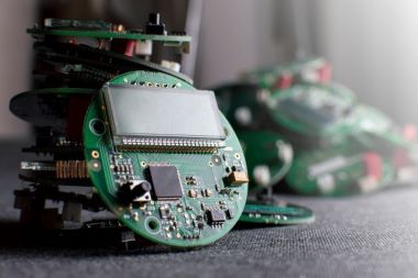
PCBS can be customized in different shapes, although square and rectangular PCBS are the most common, and as the electronics industry continues to evolve, circular PCBs are increasingly become popular. Round circuit boards are commonly used in consumer electronics, wearable devices and so on.

Advantages of round PCBS

The advantage of round PCBs is that they provide more board space. However, be very careful when making a circular PCB, as the process of making it is more complicated than that of a rectangular PCB. The fact that the wiring process of a circular PCB takes a lot of time also has an impact on the total cost of producing it.

Types of circular PCB

Circular PCB types are divided into several types according to the number of layers:

  • Single layer circuit board, widely used in low density design, commonly used in lighting field round circuit board. Such a PCB has components on one side of the board and a conductor pattern on the other.
  • Double-sided circuit board, widely used in wearable devices, electricity meters, etc.
  • Multi-layer circuit boards, with more than two conductive layers, which provide higher density and larger board space.

Circular PCB design rules

To be sure, circular circuit boards are more complex in design than rectangular circuit boards. There are some rules to follow when it comes to round boards:

1. Drawing shapes is very important when using CAD tools

2. It is best to use straight line molding around the circular circuit board

3. If it is designed for high-speed equipment, it is better to choose multi-layer design.

4. The shape of the ground plane or power plane can be defined to a large extent using the polygon editor.

5. The plate design of the circular circuit board is usually the stamp hole.

6. When assembling, a gap of 10 millimeters (about 0.39 inches) must be maintained between the round boards. However, with larger milling cutters, the clearance can be increased.

7. For the assembly of circular circuit boards, both SMT (surface mount technology) and THT (through-hole technology) can be used to place components, but SMT is more suitable for circular circuit boards.

To sum up

Although the circular circuit board design is a bit complicated, but using the right tools and following the circular design rules, help to speed up the product design process.

Working with a professional electronics manufacturer during the PCB design phase can help identify design defects without having to deal with the high cost of defects.

With over 10 years of experience in electronics manufacturing, KingPCB is fully equipped to handle your PCB manufacturing and assembly requirements. If you have any questions, feel free to contact us by email sales@kingpcb.com

Categories
PCB Blog

Why is a PCB Assembly Quote Important for Your PCB Project?

After completing your PCB design, the next step is to choose the right PCB supplier to bring your design to life.

So as a first step, it is crucial to request a PCB quote. To get an accurate quote, be sure to provide your PCB supplier with relevant information about your project.

In general, a PCB assembly service quote contains the following components.

PCB assembly service quote

In simple terms, a standard PCB assembly service quote contains two parts, one is the cost of manufacturing the board, and the second is the price of PCB assembly.

Before requesting an accurate quote, you should provide as much of this important information as possible to ensure that the price and run time estimates:

Documents required for PCB assembly quotation

Accurate quotation depends on the availability of the following documents.

Bare board printing or manufacturing drawings

It provides mainly the following information.

In addition to this, you will need to provide Gerber files, preferably in 274-x format.

Bill of materials

BOM (Bill of materials) is another important document, the more detailed it is, the better for the PCB supplier to estimate the price. The BOM sheet mainly contains information such as part description, number, reference mark, etc.

Assembly print

With assembly printing, information about the location of the parts can be conveyed.

Supplier list

Ideally a list of approved suppliers and the manufacturer’s part number can be provided.

Information often missed when requesting a quote for PCB assembly

The following is some of the information that is often omitted

Stacking

Include the number of layers, thickness, and details related to the lamination

Solder resist

Soldermask type

Impedance

For high-speed PCB manufacturing, impedance details are essential

Depanelization method

The size and location of the cutout is essential to get an accurate quote for PCB assembly

Silkscreen

Silkscreen files and color selection are also essential details

Surface finish

The type of surface finish has a significant impact on the cost

The main factors affecting the cost of PCB assembly

Mounting technology

The use of SMT (surface mount technology) or through-hole assembly will affect the cost. Compared to through-hole assembly surface mount technology is faster and more automated.

Number of layers

The cost of assembling multi-layer PCBs usually requires higher technology, so the cost is also higher.

Surface finish

As mentioned earlier, the choice of surface finish has a significant impact on cost. Some surface finishes have longer shelf life and higher cost.

Delivery time

Usually delivery time and PCB assembly cost is inversely proportional

Shipping costs

High volume PCB production means more packaging, more volume, and more shipping costs.

Explore KingPCB’s PCB assembly services

PCB assembly quotes depend on many factors, and it is important to provide us with detailed information in order to give you an accurate quote. While price is not a deciding factor in choosing a particular supplier, professionalism can be seen in a detailed and professional quotation form.

KingPCB offers reliable, high quality PCB manufacturing and assembly services, contact us now to get a quote for any type of fast PCB assembly service.

Categories
PCB Blog

The Most Common Types of Finite Element Analysis in PCB Manufacturing

The development of IoT technology has led to the advancement of printed circuit board technology as well. Miniaturization and precision are the macro trends in the electronics industry. When solving any complex problem, breaking it down into smaller parts and solving them one by one can effectively eliminate the stress caused by the problem. The technique that best defines this approach is finite element analysis, or FEA as it is often called.

What is PCB finite element analysis?

Finite element analysis techniques involve modeling a system in a virtual environment in order to solve real-world structural and performance problems.

In short, what FEA does is allow the process to be broken down into smaller subsystems so that they can be closely evaluated. One practical application of FEA is to track material changes and help with material selection. Some of the benefits of FEA include

  • Improving product performance
  • Evaluating different designs
  • Optimizing designs

Usefulness of finite element analysis for PCB manufacturing

FEA analysis can add value to different stages of PCB manufacturing in a number of ways. Examples include component selection and circuit performance. The following are detailed types of analyses applied by FEA in the design phase.

Thermal Analysis

Thermal analysis is a type of finite element analysis that is widely used in PCBs. It evaluates the board’s response to different thermal conditions, whether it is power, or thermal changes caused by environmental changes, and it helps determine the thermal conductivity pad, the use of vias and the overall thermal management design.

In addition, FEA analysis can also be useful for component manufacturers and test houses, and requires a number of tools

  • PSpice, which allows modeling of electronic components, circuits, and boards to evaluate signal response.
  • 3D Solver Clarity, which helps to provide 3D perspective and analyze EM parameters.
  • Celsius temperature solver, which provides results to ensure that no overheating occurs

Electromagnetic compatibility and integrity

EMI or noise is a common problem with boards, and the possibility of completely eliminating noise is somewhat slim, though you are still able to achieve the best EM balance for your environment. In systems with multiple PCBAs, achieving electromagnetic compatibility is an important design aspect.

Signal and Power Integrity

To ensure product reliability, the PCBA must operate seamlessly according to set benchmarks. It is primarily the signal and power integrity of the board that determines this.

  • Maximize signal-to-noise ratio
  • Components should have sufficient power
  • Noise reduction on power supply alignments

To summarize

Finite element analysis ensures that different aspects are accurately evaluated and standards are adhered to, the integrity of the PCB is checked and product reliability can be guaranteed.

KingPCB offers unparalleled quality and service for rapid PCB prototyping, domestic and offshore manufacturing, whether in the defense, industrial, medical or consumer electronics industries. Our consistently high quality, fast delivery, and competitively priced products set us apart from other suppliers.

Contact us now for more information on our PCB manufacturing and assembly capabilities!


Categories
PCB Blog

Common Failures of Discrete Components

The selection of components is one of the important steps in the PCB design process. It is worth noting some of the errors that often occur in discrete components. Understanding and paying attention to these errors will effectively help you reduce the impact that may be brought to the board assembly.

What is a discrete component?

Discrete components are the basic components of a circuit with a single function, such as transistors, diodes, resistors, capacitors, inductors, etc. Individually, they are discrete devices. They can be active or passive.

A term opposite to discrete components is integrated circuit, so what is the difference between discrete and integrated circuit?

Integrated Circuits vs. Discrete Components

Integrated circuits are basic circuit components such as transistors, diodes, resistors, capacitors, inductors, etc. made on a small wafer and then packaged to form a unit with certain functions.

The use of integrated circuits can greatly reduce the size of a circuit. However, with a limited area, it is impossible for an integrated circuit to make every part work well. Discrete components, on the other hand, consider only their own performance individually, making them more flexible.

When using discrete components, some reasons may lead to component errors.

Why do discrete component errors occur?

Common sources of errors include voltage fluctuations, component aging, overheating, corrosion, and other causes. To reduce this possibility, the following principles can be improved.

Common causes of component damage include voltage breakdown, and current burn-in. In this article, we will focus on common causes of electronic component failure such as capacitors, resistors and inductors.

Common Causes of Capacitor Failure

Capacitors are used in various applications such as: filtering, decoupling, impedance matching, bypassing, etc. The causes of capacitor failure are:

  • Overload currents and voltages
  • Temperature variations
  • Dielectric failure

Signs of capacitor failure

  • Oil leakage
  • Deformation due to internal fluid leakage from overheating
  • Scratching of wires
  • Protruding cap, rupture, etc.
  • Increase in capacitor temperature

Common causes of capacitor failure

Resistors are mainly used in circuits to regulate and stabilize current and voltage, as shunts and voltage dividers, and also as circuit matching loads. Causes of resistor failure include

  • Shock and vibration
  • Dust buildup, ambient humidity, insulation problems, etc.
  • Aging
  • Overheating can cause open circuits in wirewound resistors
  • Resistor material problems

Causes of inductor failure

Inductors in the circuit mainly play a role in filtering, oscillation, delay, trapping, etc. The most common role of inductors in the circuit is to work with capacitors to form LC filter circuits. Capacitors have the characteristic of “blocking DC, passing AC”, while inductors have the function of “passing DC, blocking AC”.

Thermal stress due to open circuit is one of the main causes of inductor failure. Overheating inductors are mainly characterized by shorted coils. Current spikes and melting of the insulator.

To summarize

It is critical to consider these failure modes before selecting components for your board.

Choose an exprienced PCB manufacturer for your PCB project that can provide high quality and reliability, KingPCB is fully capable of meeting your PCB manufacturing needs.

Contact KingPCB now for a free quote with PCB file inspection.

Categories
PCB Blog

How to Meet Standards for EMI and EMC for PCB Design?

Electromagnetic interference (EMI) is closely related to our lives. For example, when you use a wireless network, while using a microwave oven, you will feel some influence of radio signals; in the airplane was asked to turn off electronic devices and other situations.

Due to the huge number of electronic products, the impact of EMI must be taken into account.

What is EMI and EMC in PCB?

EMC is the ability of an electronic system to operate in an electromagnetic environment without generating EMI or electromagnetic interference.

EMI is electromagnetic interference or disturbance, which disrupts signal quality and causes equipment to malfunction when energy is transmitted from one electronic device to another.

What is EMC/EMI standards in PCB design?

The goal of EMC/EMI standards is to maintain compatibility between electrical and electronic systems in the same location for trouble-free operation.

Two types of requirements of EMC/EMI: regulatory standards and industry standards.

EMC regulatory standards vary from region to region. Early EMC standards were developed by the US Federal Communications Commission. The European Community later developed its own EMC standards, known today as the EMC Directive.

Industry standards, on the other hand, are defined by industry and can ensure operability and uniformity.

Broad requirements for compliance with EMC standards

Electronic circuits consist of multiple electronic components arranged in a predetermined manner. If not arranged properly, they can lead to various EMI/EMC problems. In order to comply with EMC standards, designs need to meet the following aspects.

  • EMI immunity design. Attention to proper stacking and wiring strategies.
  • Equipment radiation control. Need to ensure that the equipment emits the least amount of radiation, for PCB stacking, component placement, grounding design strategies, etc. to optimize.
  • Suppress conducted EMI. conducted EMI can take many forms, such as switching noise from SMPS regulators, coupled common-mode noise, etc.
  • Pay attention to transients or power fluctuations. This may be in the form of buck, power spikes, etc.
  • Surge and ESD design.

What does EMC testing consist of?

EMC test includes EMI and EMS two parts, EMI test content is mainly the following items

  • Radiated Emission
  • Conducted Emission
  • Harmonic
  • Flicker

Effective strategies to help pass EMC standard tests

Lamination, Power and Grounding

PCB designs use low inductance grounding systems to minimize EMI. multilayer PCBs place ground layers below signal layers to minimize loop inductance.

Shielding

The simplest method is to use ground shielding to form a Faraday cage around sensitive components and alignments. Some common types used to always radiate EMI are

Differential pairs

Use differential protocols to route signals whenever possible. Compared to ordinary single-ended signal routing, differential signals have the advantages of high interference immunity, effective EMI suppression, and precise timing positioning.

Mixed-signal and layout routing

It can be a good separation of the digital, low frequency analog and RF analog parts of the board.

Decoupling capacitors

It is recommended to use bypass/decoupling capacitors between the power supply pins of active components and the ground cross-hole. This ensures that residual noise is passed to ground.

To summarize

The EMC bucket of any electronic circuit is related to the generation, propagation and reception of electromagnetic noise. It is important to use the right tools and the right expertise to design PCBs so that they comply with EMI/EMC standards. The right PCB assembly partner can create compliant layouts and also perform any rework.

If you have any requirements or urgent help with PCB fabrication, kindly send your inquiry by sales@kingpcb.com or contact us through our contact page.

Categories
PCB Blog

Vias in BGA Pads

Have you ever considered using Via-in-pad when designing your PCB?

Via-in-pad designs are becoming increasingly popular, and if you are unsure whether to use a printed circuit board with traditional vias or vias in pads. This article will take you through what vias in pads are.

What is a Vias-in-pads?

This is an in-pad vias design, which is simply a via under the pad.

The vias in the tray is mainly used for BGA packaging area, because its surface needs to be soldered or chip paste. The requirements for its accuracy and acceptable area are high, as is the surface flatness to prevent false soldering or bad nodes due to uneven chip placement.

Advantages of the vias-in-pads

VIA-IN-PAD, also known as VIP design, the main advantage is that it reduces the area required for vias, making it easier to manufacture miniaturized PCBs and significantly reducing the board area required for signal routing.

By connecting the vias directly to the layer below the component, you can route signals without going outside the device package.

Traditional Through-Hole vs. vias-in-pads

In a traditional PCB via layout, you can use a solder resist layer to prevent solder from entering the via and avoid electrical connection problems.

When you use vias-in-pad, the practice of using traditional via will not work and the via-in-pad must completely fill the via so that there is no air trapping and degassing.

Typically, PCB manufacturers fill the through-holes in the pads with epoxy after they have been mechanically drilled and plated. Or, you can laser ablate your vias and fill them with copper. What you choose to do will depend on your specific application and the needs of the printed circuit board and the size of the vias. The main issue that determines the process is the pad diameter.

Choosing traditional vias or vias-in-pads?

With the development of lighter, thinner and smaller electronic products, PCBs are pushing towards higher density and more difficult development, so the size of the components is getting smaller and smaller. With small pin spacing, it is difficult to wire the pins inside the package, so it is necessary to change the layer of hole punching wiring.

In the case of sufficient spacing, it is suggest that not use the vias-in-pads design, because the manufacturing of vias-in-pads high cost, production cycle time is also longer.

Explore KingPCB’s PCB over-hole manufacturing technology

KingPCB has extensive experience in printed circuit boards, whether it is blind vias, micro vias, or plate vias, we can provide you with high quality services.

Contact us now for more information about our PCB manufacturing!


Categories
PCB Blog

How to Overcome the PCB Electromagnetic Problems

Electromagnetic problems are a problem that PCB designers must face. Simply put, even small design issues can lead to electromagnetic problems, and system design engineers must always monitor electromagnetic compatibility and interference.

What are the PCB electromagnetic problems?

PCB electromagnetic problems relate to EMI and EMS, which usually includes the generation, propagation, and reception of electromagnetic energy processes.

EMI (Electromagnetic Interference)

Refers to the work of electronic products that will cause interference with other electronic products in the vicinity, with which there are EMC specifications.

EMC (Electro Magnetic Compatibility)

It means that the electromagnetic energy generated by the device neither interferes with other devices, nor the ability to interfere with the electromagnetic energy of different devices.

Any PCB designer should follow the EMC design rules to minimize the number and impact of EMI.

Classification of electromagnetic interference sources

With the development of modern electronic technology, electromagnetic interference has become ubiquitous, we can classify it from the following aspects.

  • Sources

They are divided into man-made interference and natural causes. Man-made electromagnetic interference from electronic circuits, natural effects may come from the universe, atmospheric lightning,  and other environmental factors.

  • Duration

Continuous interference emits a constant signal, it is also a source of EMI, usually manifested as background noise. Pulse interference is intermittent, usually caused by switching systems, lightning, and other non-constant sources.

  • Bandwidth

Narrowband signals used by radio may encounter interference from oscillators and transmitters, broadband interference affects high data signals such as television and can come from many sources, including arc welders and solar noise.

What are the effects of electromagnetic interference?

Whether human or environmental, EMI can be dangerous. For example, in the medical field, the use of wireless devices is being born, unfortunately, EMI can affect the function of medical equipment such as ventilators, ECG monitors, and heart monitors.

In other industries, EMI can break the loop of sensors and navigation systems, causing data to be biased and thus leading to the wrong results.

The most common source of EMI is the internal design, poor PCB design can lead to incompatible signals on the board, which may eventually lead to board failure

How to prevent and solve electromagnetic problems?

To minimize EMI, PCB designers must follow EMC design principles. EMC problems are mainly related to design flaws that cause interference between alignments, circuits, vias, PCB coils, and other components.

Grounding plane

The design of the grounding layer is critical to reducing EMI. This is because all circuits need to be grounded in order to work.

  • Maximize the grounding area within the PCB
  • Use a solid ground plane
  • Connect each component to a ground plane or point
  • Use split planes carefully
  • Connect bypass or decoupling capacitors
  • Minimize signal length

Alignment layout

Proper use of traces ensures proper propagation of current. Traces are essentially conductive paths that contain flowing electrons when the circuit is active, and simple bends or crossings can cause PCB EMI.

  • Avoid right-angle designs
  • Separate signals
  • Shorten the current return path
  • Keep spacing between traces to a minimum
  • Be careful with vias design

Component Alignment

Some best practices for component layout in PCB design include:

  • Separate analog and digital components
  • Separate analog circuits and high-speed trace sections
  • Beware of high-speed components

EMI shielding

Small, high-speed components will always generate some EMI; fortunately, shielding and filtering can minimize the impact of this EMI.

  • Component and board physical shielding
  • Low-pass filtering
  • Cable shielding

Explore KingPCB’s PCB manufacturing and assembly services

King PCB is the industry’s leading supplier of circuit boards and we manufacture your PCB projects in China. Our goal is to provide our customers with the best PCBs with high quality, fast delivery, and competitive pricing.

If you need to manufacture a unique type of circuit board, our professional team can help you find the right surface finish, vias, and assembly techniques to achieve your best PCB project.

Let us help you realize your project, contact us now for a quick free quote!

Categories
PCB Blog

PCB Layer Stacking Capabilities

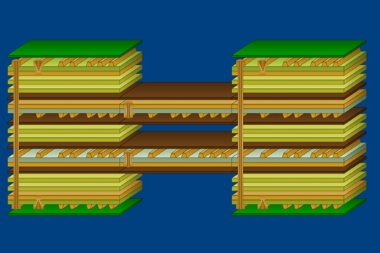
As circuit boards become more complex, bringing more functions and circuits together on a single board, compact PCB layouts need to provide more functionality. Therefore PCB is gradually moving to multi-layer PCB stack design, so what is PCB stack? And how do they work?

What is a PCB stack?

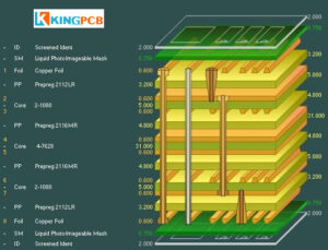
PCB stacking is a stack of copper and insulation layers that make up the PCB. In the most basic case, multi-layer PCB consists of at least three conductive layers. The bottom layer is synthesized with an insulating board, and each layer of the board is connected to the next.

Advantages of PCB stacking

  • Improved functionality

Multi-layer PCBs can exponentially increase the speed and functionality of a device, resulting in a more powerful board

  • Protection of internal layers

Layer stacking can help protect internal layers from external noise

  • Reduces radiation

In high-speed layouts, PCB layer stacking can help you minimize radiation from your equipment. However, you need to be aware of impedance mismatches, which can lead to greater EMI emissions than with a normal PCB

  • Reduce Cost

Good PCB stacking can help achieve low cost manufacturing by placing multiple circuits on a single board

How to create multilayer PCB stacks

Multi-layer PCB stacks should achieve the following minimum objectives through careful design to meet specific design requirements.

  • Ground and power layers should be tightly coupled together
  • Signal layers are adjacent to the plane
  • High-speed signals are transmitted through the buried inner layer to control radiation
  • Include multiple ground planes to reduce impedance and radiation
  • Signal layers are coupled as close to their planes as possible

It is important to note that not every PCB stack can meet the above objectives; in fact, only an 8-layer board can meet all five objectives. You should work closely with your PCB engineering team to determine which goals are the highest priority for your PCB stack.

Common PCB layer stack types

There are five types of PCB layer stacks – 2-layer, 4-layer, 6-layer, 8-layer, and 10-layer. Exactly how many layers you need depends largely on the size of the circuit, the size of the board, and the board’s EMC requirements. From there, you can determine the layout of the board.

2-Layer PCBs

Often referred to as a double-sided PCB, it is the most common type of PCB. A double-sided PCB consists of three material layers.

Signal layer, which consists of copper and is approximately 0.0014-0.0021 inches thick

– Laminated core, separating the top and bottom copper layers, with vias to create connections between the two sides of the board.

– Bottom, second layer of copper similar to the signal layer, thickness of about 0.0014-0.0021 inches

4-layer PCB

In terms of PCB stacking, 4-layer PCB is the second most common choice for multilayer boards. However, the inner layers of a 4-layer PCB cannot be connected externally, so they are often used as power planes or for signal routing, which helps improve the quality of the alignment signal and reduces EMI emissions.

– Top Layer

Prepreg

– Inner Layer 1

– Core board

– Inner Layer 2

– Prepreg

– Bottom layer

6-Layer PCB

6-layer PCB is functionally a 4-layer PCB with two additional signal layers

– Top layer

– Prepreg

– Grounding layer

– Core board

– Route layer

– Prepreg

– Route layer

– Core plate

– Power plane

– Prepreg

– Bottom layer

8-Layer PCBs

The 8-layer PCB stack offers more options than a 6-layer board by adding two layers for routing or performance. It is also the first board to market that achieves all five goals of a multilayer PCB design.

– Signal Layer 1

– Prepreg

– Grounding layer

– Core board

– Signal layer 2

– Prepreg

– Power plane

– Core board

– Grounding layer

– Prepreg

– Signal layer 3

– Core board

– Power plane

– Prepreg

– Signal layer 4

10-Layer PCB

If your design requires six wiring layers, then you should look at a 10-layer board.

– Signal layer 1

– Grounding layer

– Signal layer 2

– Signal layer 3

– Power plane

– Ground plane

– Signal layer 4

– Signal layer 5

– Power plane

– Signal Layer 6

KingPCB-Your source for quality multilayer PCBs

If you need to add functionality to your PCB, multilayer PCB lamination is a great option. No matter how many layers you need, KingPCB can help you.

KingPCB is located in Shenzhen, China and is one of the leading PCB manufacturers in China. Our high quality delivery and fast response makes us stand out from other suppliers. We also provide rigid-flex PCBs, flexible PCBs, HDI boards and other PCB related products.

Contact us now for a free inspection and quote for your multilayer PCBs.

Categories
PCB Blog

PCB Trace Impedance

What is trace impedance?

In a printed circuit board, the circuit alignment is done by copper. Copper is the least resistive element other than silver. Unlike resistance, impedance is based on frequency.

All wires and alignments will have at least some impedance to the current flowing from any driver. Often, when signals require fairly fast rise times, alignment impedance is an issue that needs resolving.

Let’s learn how trace impedance works and how to determine PCB trace impedance.

The working principle of trace impedance

Each trace has a tiny to almost indistinguishable series inductance distributed along the trace, which is inversely related to the cross-section of the trace. As the signal rise time increases, the effect of the resulting impedance becomes more pronounced.

Your driver reads all traces as distributed LC circuits, and your trace AC impedance comes from that distributed LC circuit. This is considered to be uncontrolled impedance.

No effort has been made to design the trace environment to account for this impedance, thus allowing inductance and capacitance to vary as the trace changes. Since synthetic impedance usually has no effect on operation, there is no need to waste time or money designing a way to control it.

Controllable Impedance

Considering the impact that impedance can have, designers can design a board where the alignment looks like a transmission line so that reflections can be avoided by terminating it in its characteristic impedance.

When controlling impedance, one needs to ensure that the impedance is constant at each point on the alignment, rather than varying from point to point as it would in the normal case of uncontrolled impedance. We need to control three characteristics of the circuit structure.

  • Trace width
  • The spacing between the signal return path and the signal traces
  • The dielectric coefficient of the material around the trace

You can change these geometric features and still maintain the controlled impedance, as long as you change the other features as needed so that the relationship between these aspects does not change and the impedance remains the same.

How to Calculate PCB Alignment Impedance

To create a controlled impedance PCB, you must be able to measure the impedance. The best way to calculate trace impedance is to use a trace impedance calculator. You can find the trace impedance calculator online or in your CAD software. There are several parameters to consider when determining impedance, including

  • Trace width
  • Trace thickness
  • Laminate thickness
  • Dielectric thickness
  • Copper weight

Typically, impedance can be measured using a network analyzer, laboratory time domain reflectometer (TDR), or a controlled impedance test system using TDR technology. Engineers with experience using controlled impedance test systems will run impedance tests to ensure high quality results.

Explore KingPCB’s Controlled Impedance Printed Circuit Board services

To receive information about impedance boards or to order PCBs for your industry, contact KingPCB today.

Categories
PCB Blog

Choosing Matte Finish or Glossy Finish for PCB Design?

Solder resist is a factor you must consider when it comes to creating a circuit board. You may be wondering whether to choose a matte finish or a glossy finish. In most cases, people ordering PCBs will leave the decision up to the PCB manufacturer, who usually defaults to a glossy finish.

What is a glossy finish for PCBs?

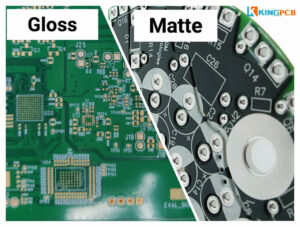
A PCB glossy finish is a reflective solder resist layer that is lighter in color than a matte finish and has a non-porous appearance.

What is a matte finish for PCBs?

As the name implies, the matte finish PCB surface is not glossy, looks darker than the glossy finish, and has a soft, porous appearance.

Functionally, glossy PCBs and matte PCBs have the same characteristics, and the difference between the two finishes is small. Which one to choose depends on the customer’s aesthetic preference.

What are the advantages of choosing a glossy finish PCB?

– Classic appearance. Since glossy solder resists are the default choice as a solder resist layer, many consider them to be the classic PCB look

– Appearance wear. The reflective nature of glossy PCBs tends to make signs of wear look less obvious

– Scratch resistance. Glossy PCBs have higher scratch resistance than matte PCBs due to their harder surface

Many people think the glossy finish looks better, it’s shiny and reflects light making it look lighter. If you want the appearance of the PCB to have a positive impact on the assembler or end customer, you can choose a glossy PCB finish.

What are the advantages of choosing a matte finish for PCBs?

– Easy to inspect. Due to the matte non-reflective properties, you can more easily view the PCB details

– Reduced solder balls. Studies have shown that lower gloss levels on PCBs result in lower levels of solder balls

While the cost benefits of choosing matte or glossy are similar, you may prefer a matte finish if you consider the impact of the solder ball factor.

One of the causes of solder ball formation is surface roughness. The smoother the surface, the more likely the solder is to ball up. If you want to simplify production as much as possible and ensure more accurate checking out of PCB errors, you can choose a matte finish.

Explore KingPCB for more information on solder resist options!

For more information about PCBs, contact us now or send emails by sales@kingpcb.com!

Categories
PCB Blog

How PCB Smart Manufacturing Overcomes IoT Challenges

The Internet of Things, also commonly referred to as the fourth revolution, is expected to have approximately 27 billion connected IoT devices by 2025, as supply constraints ease and growth accelerates further.

One such skeleton that all electronic devices have is the printed circuit board. As electronic devices are gradually miniaturized and sophisticated, how do printed circuit boards go about overcoming these difficulties?

In the face of the Internet, some of the common challenges in PCB manufacturing

  • Space constraints
  • Product fitting
  • Wearable products
  • Power consumption
  • Wireless connectivity
  • Reliability
  • High tensile strength

Space constraints

Faced with the growing space problem, rigid-flexible PCBs and HDI PCBs offer excellent solution ideas. They allow for more dense component placement, thus saving valuable space. The use of rigid-flex PCBs can offer more possibilities for mobile device installation. Some of the advantages they offer are

  • Improved design space
  • More dense circuitry
  • Weight reduction (in fact, they can reduce weight by up to 95%)
  • Increased speed and reliability
  • Adaptability to different environments

Product fitting

Virtual prototyping can go a long way toward keeping the design in sync with the form of IOT it is targeting. Often, PCB designs also require the use of non-traditional materials that contribute to functionality, such as mesh or plastic.

Wearable Products

PCBs for wearable product designs need to budget for environmental factors, and to overcome this challenge, smart PCB manufacturing can rely on comprehensive simulation testing.

Power Consumption

As IoT devices continue to communicate with the Internet, battery life and battery capacity are worthy of attention. PCB designs therefore need to keep energy usage within the circuit within a strict budget.

Wireless Connectivity

IOT PCBs add the requirement for wireless Internet access, and proper installation using wireless modules and RF circuit components helps to mitigate the challenges.

Reliability

With the development of technology, IOT applications in the continuous penetration of different industries, such as the need to work in harsh and extreme environments, to ensure reliability and durability is not a small challenge, can be tested through a large number of simulation software simulation PCB.

To summarize

The IoT industry continues to evolve although it brings many challenges to PCB manufacturing, we need to pay more attention to the relationship between the product and its PCB form.

Close collaboration between designers and engineers throughout the design process can help achieve smart PCB manufacturing, and there is no doubt that PCB design methods will continue to evolve rapidly, maximizing reliability and reducing errors will be the rallying cry for all PCB designers.

Explore KingPCB’s IoT PCB manufacturing solutions

KingPCB, one of the leading PCB manufacturers in China, has over 10 years of experience in PCB manufacturing and assembly.

High quality, efficient communication, and fast delivery capability make us stand out, and our large portfolio of satisfied customers makes the greatest testimony to our success.

Stay in touch with us anytime by email sales@kingpcb.com, or submit your request via the contact page!

Categories
PCB Blog

Why Via Tenting is Important in PCB Manufacturing?

If you have ordered and used PCBs, you have probably heard of the use of vias in printed circuit boards. Vias play an important role in the connections between the layers of the board, and they serve two main purposes.

  • Electrical signal conduction
  • Heat dissipation

In many cases, the through-hole is copper-plated. Some PCB manufacturers believe that these holes should not be exposed, when the vias are completely covered, called filled vias. There is another popular method of tenting vias.

What is PCB Via Tenting?

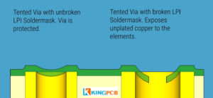
As the name implies, tenting vias means creating a tent-like shape on the vias. Tenting a vias means covering the toroid and vias with a solder resist layer, primarily covering the toroid to prevent exposure to components and reduce accidental shorts or contact with the circuit. Whether to use tenting in PCB manufacturing depends on the design of the board.

Why is PCB Via Tenting important in PCB manufacturing?

There are several ways to protect printed circuit boards from vias. For cost reasons, tented vias are usually preferable to epoxy filling. Most forms of tenting are LPI (liquid imagerable solder resist). PCB solder resist protects copper traces from oxidation, damage and solder bridging, which also applies to over-hole protection.

If your PCB is designed with a through-hole assembly, the tent through-hole will prevent solder from flowing up into the through-hole and over the other side of the PCB when using wave soldering.

The vias near the SMT pad should also be tented. This will prevent the solder paste wick from sucking into the via hole and creating a bad solder joint.

Disadvantages of PCB Via Tenting

Since the LPI solder resist is a liquid, it must “bridge” the gap above the via. This results in the solder resist not completely covering the via, leaving a small hole.

These small holes can be used for corrosive fluxes, moisture and other chemicals to enter the vias. This can lead to failure due to corrosive vias.

This is not an issue due to the popularity of no-clean flux in SMT assembly, but corrosive water-clean flux is still prevalent in through-hole assembly.

Under what circumstances is PCB Via Tenting used?

Whether to use Tenting depends firstly on the PCB design, and secondly on the size of the via.

Tenting vias are suitable for through-hole diameters of 12 mil or smaller. If you are dealing with larger vias, using filled vias is a better option, it is relatively more costly.

Contact KingPCB for PCBs with tented or non-tented vias

At KingPCB, we have experience with almost all types of printed circuit boards. We can help you find boards in a variety of materials, in flexible or rigid-flexible formulations, with tented vias, filled vias, blocked vias, open vias, or a combination of these.

Our high quality manufacturing, ability to deliver, and quick response sets us apart!

Contact us now to get more information about our PCB manufacturing capabilities!