Categories
PCB Blog

Key Factors Affect the Cost of Multilayer PCB Assembly

The application of multilayer PCBs is becoming more and more common.

There are many factors that determine the cost of manufacturing multilayer PCBs, which are mainly divided into the following categories.

  • Material
  • Size
  • Number of layers
  • PCB thickness
  • Surface treatment process
  • Hole type and number
  • Alignment width and spacing
  • Other special process requirements

Materials

The choice of what material to manufacture PCBs has a significant impact on the cost, in the selection of substrates for multilayer PCBs, here are a few points to consider.

  • High and low temperature requirements. For boards that need to operate under high temperature conditions, the need to use high TG material (TG that is, the glass transition temperature point)
  • Signal performance. The choice of material depends on the advantage of being able to provide uninterrupted electrical signals.
  • Mechanical properties.

Size

PCB costs are calculated by size, so the larger the PCB size, the more material required and the cost will increase. But this does not mean that the smaller the size of the cost is less, the processing time involved in small size PCB will also affect the cost.

Number of layers

The number of layers is another major determinant of the cost of multilayer PCBs. For the more layers of PCBs, the more resources and time required for the manufacturing process, the higher the cost.

PCB thickness

PCB conventional thickness is 1.6mm, for thicker materials are usually more expensive in production, lamination and PCB made.

Surface treatment process

The choice of surface finish treatment is critical to improving PCB reliability and shelf life, KingPCB default PCB manufacturing surface treatment is HASL, when it comes to HDI PCB, ENIG may be required, which also has an impact on the cost.

Hole type and quantity

The price of multilayer PCB manufacturing is closely related to the through hole

  • Hole size (conventional holes greater than or equal to 0.3mm)
  • Hole type (whether it involves micro vias, blind vias, buried vias)
  • Quantity (general hole density is not greater than 100000/㎡)

Alignment width and spacing

Multilayer board needs better heat dissipation ability, in order to avoid overheating, need to have enough alignment width. If you expand the alignment width or add extra solder, it will increase the material cost and workload.

Other special process requirements

Some other factors that may affect the cost are impedance control, ink, depth control, halogen-free materials, ink plugging, copper thickness, etc.

Explore KingPCB’s multilayer PCB assembly services

There are many factors that affect multilayer PCB manufacturing and assembly, please be careful when making any budget decision for multilayer PCB assembly.

KingPCB, one of the leading PCB manufacturers in China, uses modern technology and advanced equipment to provide you with PCB assembly services.

If you are looking for a multilayer PCB manufacturer or would like to see a quote for your project, contact us now for a quick quote!

Categories
PCB Blog

Wave Soldering and Reflow Soldering: Which is Better for PCB Assembly

Soldering is an important part of the printed circuit board manufacturing process. The reliability of a circuit board is achieved by sticking electronic components to your board through soldering. Wave soldering and reflow soldering are common soldering methods for PCB assembly.

Each method has its advantages and disadvantages, and this article will walk you through their meaning and application.

What is wave soldering?

Wave soldering is a batch soldering process that allows many boards to be manufactured in a very short period of time.

It is called “wave soldering” because the soldering surface of the plug-in board is in direct contact with the high-temperature liquid tin, which maintains a sloping surface, and a special device makes the liquid tin form a wave-like phenomenon.

Wave soldering process

  • Insert the component into the corresponding hole
  • Pre-application of flux
  • Preheat (90-100 ℃)
  • Wave soldering (220-240 ℃)
  • Cooling
  • Cut off excess plug-in pins
  • Inspection

During the wave soldering process, it is worth noting that proper temperature is very important. Failure to adequately control the temperature may result in cracking and electrical loss.

Wave Soldering Disadvantages

  • Solder consumption
  • Flux consumption
  • Nitrogen consumption
  • Power consumption
  • Need for solder rework after wave soldering
  • Need to clean wave solder holes and solder components

What is reflow soldering?

Reflow soldering is different from wave soldering and is commonly used to solder surface mount components. It is refers to the use of solder paste (a mixture of solder and flux) to connect one or more electronic components to a contact pad and then melt the solder by controlled heating to achieve a permanent bond.

Reflow soldering process flow.

  • Apply pre-solder paste
  • SMT (manual or automatic machine placement)
  • Reflow soldering
  • Inspection and electrical test

Wave vs. reflow soldering

The choice of which type of soldering to use depends on a variety of factors, such as pad shape, component orientation, PCB type, etc.

For printed circuit boards with through-hole components and larger surface mount components, wave soldering is an ideal method.

However, in some ways, wave soldering is more complex and requires careful monitoring of issues such as board temperature and the time the board spends in the solder wave. Failure to create the correct wave soldering environment is more likely to result in board defects.

When using reflow soldering to manufacture printed circuit boards, you don’t need to worry about controlling the environment.

To sum up, wave soldering is faster, cheaper, and cost-effective for high-volume orders. Reflow soldering is typically used for small-scale manufacturing products that do not require a method suitable for fast, inexpensive mass production.

Explore KingPCB’s PCB assembly services

The type of soldering is just one of the many elements of PCB assembly. Choose your soldering partner wisely, research carefully for your requirements and provide a soldering process that works for you.

KingPCB is very knowledgeable about solder types and other elements of PCBs, such as types of substrate materials, board variations, and important design features.

To learn more about KingPCB’s fabrication and assembly information, contact us now!

Categories
PCB Blog

FAQ of Flexible PCB

Flexible PCBs are a great innovation in the field of printed circuit boards. Flexible circuit boards are made of polyimide or polyester film as the substrate.

They are suitable for different electronic applications with their excellent flexibility. It has the characteristics of high wiring density, light weight, thin thickness and good bendability.

However, you may find that there may be some problems when using flexible circuit boards.

Why is there a problem with flexible printed circuit boards?

Because flexible PCBs are designed and manufactured for special applications, the cost of starting circuit design, wiring and photographic backing is higher.

In most cases, flex PCB problems occur because designers are used to designing rigid circuit boards, so they design flex PCBs based on the same principles. Of course, flexible circuit boards are not rigid circuit boards, they need their own flexible design.

What are the common flexible circuit board problems?

Stacking traces

It is important to ensure that copper stays on the neutral axis of the bend. When traces on either side of a dielectric stack overlap each other, the traces on the outside of the bend radius will usually break when the circuit is bent if the traces on opposite sides are perfectly aligned.

The farther the tension moves these traces away from the neutral axis of the folded region, the greater the likelihood of breakage.

By designing this area as a conductive layer, you can sidestep this problem.

Stress points in the conductor

At the bottom of the pads or sharp corners of the board with sharp bonding points, this situation does not apply to flexible boards but rigid boards. Because whenever the user bends the area where the stress point is located, there may be fractures or delamination.

Spacing between solder pads

It is important to ensure that the flexible circuit board you design has more space between each pad and its adjacent conductive traces to account for larger overlay openings. If the distance is too short, the result may lead to a short circuit between the connector pads and pins.

Solder joints too close to the bend point

Solder joints are the points where the solder is bonded to the copper traces. Due to the addition of solder, they are harder than the rest of the copper traces. In flexible boards, if the solder joints are too close to the bend point location will likely lead to pad breakage or loss of lamination, resulting in board damage.

Solder resist/overlay openings are not wide enough

The shape of the flex circuit may change somewhat during the manufacturing process. There are many complex processes to consider when designing a custom flex circuit, so it is important to make sure the openings in the overlay are wide enough.

How can I avoid problems?

To avoid problems with flexible circuit boards, it is important to get to the root of the problem – the design

Explore KingPCB’s Flex PCB Services

If you need flexible circuit boards, rigid circuit boards or flexible-rigid combination boards, KingPCB is your reliable choice. We are one of the leading PCB manufacturers in the printed circuit board industry looking for the best design and manufacturing.

For more information and quotes on flexible circuit boards, contact us today!

Categories
PCB Blog

OEM PCB Manufacturer Box Build Assembly Services

PCB box build assembly is very beneficial when producing electromechanical devices. You will see many advantages when you choose a PCB manufacturer that is reliable and has extensive manufacturing experience. They help you to reduce your production costs without causing any defects to your product.

What is PCB box build?

Also known as system integration, a boxed build is a combination of circuit boards, cables and wires, subassemblies, and finally, case fabrication.

Once it is fully completed, the assembly is a finished product that operates as intended with a practical enclosure that meets the needs of the application.

The process of PCB box assembly involves

  • Fabrication of the PCB
  • Assembly of the PCB
  • Connection of component wires and cables

Choosing the right enclosure is critical to the success of your electronic equipment, whether it is part of a wireless industrial control, medical device, or energy distribution system.

PCB Box Build Design Guidelines and Best Practices

Proper box build design will ensure the long-term success of your electronics project. Once you have identified your electronics contract manufacturer, you must provide them with a variety of information to continue your work. You should provide them with all the essential information they may need.

The strategy for PCB box builds can be boiled down to

  • Size
  • Material
  • Transmission
  • Layout
  • Compatibility
  • Testing requirements


Confirm proper dimensions

Use 3D modeling to create a perfect-fitting enclosure. Size is an important part of the final product, and the size and weight of the product will be one of the most important factors affecting shipping costs.

  • Packaging
  • Shipping
  • Storage

As a general rule, it is more difficult to build the right enclosure if the device is larger. Work with your product development team to ensure that the size of your equipment meets manufacturability design requirements.

Select the right enclosure material

When building for a PCB box, consider the following factors when selecting the right material.

  • Durability
  • Ductility
  • Usability
  • Cost
  • Application requirements: environmental factors

Ensure adequate signal transmission

Metal enclosures may impede the transmission of wireless signals. Plastic enclosures are more suitable for wireless devices, but when used in extreme temperature environments, metal enclosures are still preferable.

Choose a thoughtful layout and design

In understanding the audience of your product, consider the brand theme of the product to design the appearance of the product.

Compare CAD with BOM

Compare your CAD with the BOM (Bill of Materials) before going into production to ensure package compatibility. The bill of materials is like a blueprint for PCB boxed assemblies, which provides information on

  • Package
  • Reference number
  • Item number
  • Part type
  • Manufacturer part number, etc.

Test Requirements

You must inform the PCB manufacturer of your requirements for product testing; you can also ask your PCB supplier for available test methods first. The conventional test methods are

  • Functional testing
  • Basic electrical testing
  • Aging testing

Why choose PCB box build assembly service?

Success with PCB box build assembly services can be achieved in a number of ways. PCB box build services help integrate PCB systems in two different ways: the fabrication of the PCB and the installation and its wire connections.

Providing detailed information about your manufacturing requirements to your PCB partner ensures your success with PCB box builds.

Explore KingPCB’s box build services

As one of the leading PCB manufacturers in China, KingPCB offers customized PCB electronics box build and system assembly services with advanced technology. Request a Box Build Assembly quote contact us now!

Categories
PCB Blog

Which Works better? Thermal Pad vs. Thermal Paste?

With the miniaturization and intensification of electronic products, how to effectively dissipate heat has become a matter that PCB manufacturers need to face.

Thermal Analysis

Effective thermal management requires a detailed thermal analysis.

Thermal analysis assists designers in determining the electrical performance and reliability of components on the PCB, helping to determine whether components or PCBs will fail or burn out due to over-temperature function.

A simple thermal analysis simply calculates the average temperature of the PCB, while a complex one models the transients of electronic devices containing multiple PCBs and thousands of components.

PCB thermal management design practices

There are several thermal methods that can be used when designing and prototyping PCBs.

To ensure a good connection between the IC and the heat sink, thermal pads and thermal paste are often used.

What are thermal pads and paste?

Thermal pad

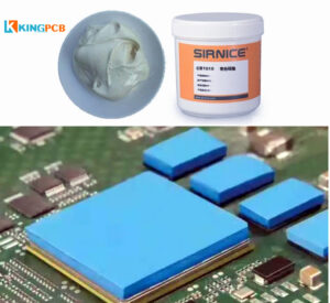
Thermally conductive pads are made of thermally conductive materials that are inherently sticky, soft, good compression properties, and excellent thermal conductivity. They help to dissipate heat easily when placed between the component and the heat sink.

What are the advantages of thermally conductive pads?

  • Easy deployment
  • Flexibility to cut to any size
  • Multiple material options

Thermal Paste

Essentially, thermal paste performs the same function as a thermal pad. The thermal paste works by closing any air gap between the heat generating component and the heat sink. This ensures that the air gap does not act as a thermal insulator and that heat is easily dissipated.

What are the advantages of thermal conductive paste?

  • Price advantage
  • Easy to apply, fills uneven gaps and provides a thinner interface, thus providing better thermal conductivity
  • Durable and more robust

Choose thermal pad or thermal paste? Which works better

The truth is that no one choice is absolutely perfect. Each material has its advantages and disadvantages, and the choice depends on the application requirements of the product. All we need to do is to carefully evaluate the thermal requirements of the board and then choose the most suitable material.

In addition to using thermal pads or thermal paste, you also need to use appropriate through-hole and surface mount pads, alignment wiring, and power layers for your IC design. This will greatly help you to manage the thermal condition of the board.

Explore KingPCB’s manufacturing services

In essence, thermal management is a technique used by PCB manufacturers.

KingPCB as one of the leading PCB manufacturers in China has over 10 years of experience. It is our goal to adhere to strict high standards of PCB manufacturing and assembly.

To get a fast PCB manufacturing quote, contact us now!

Categories
PCB Blog

Rapid PCB Prototyping-How to Pick An Appropriate Manufacturer?

When developing a new product, each idea need design, built and test, and most developers use prototyping for this purpose.

Prototyping is an important part of the design process, but it also faces some challenges, as many manufacturers do not accept small orders, resulting in increased product design time and time-to-market.

Rapid printed circuit prototyping can solve this problem.

What is Rapid PCB Prototyping?

PCB prototyping focuses on functional design with the primary purpose of testing to meet the functional requirements of the project. And it is possible that the PCB prototype is not the final form of the product. Rapid PCB prototyping is characterized by speed, which helps to shorten the design and testing process.

Differences Between Prototypes and Final Products

  • Materials:

The materials used in the final product may be expensive or not easily manufactured, so prototypes are made with materials different from the final product. Sometimes even the materials for the final product are still under development and not yet available for use in prototypes.

  • Process:

Mass production does not lend itself to making small quantities of parts, so prototypes may be made using a different process than the final product. For example, a final product made by plastic injection molding requires expensive molding tooling, and prototypes can be made by machining or 3D printing to save money.

  • Validation:

The final product may require several quality tests to verify compliance with the design or specifications. Some adjustments or rework are usually assumed as part of the manufacturing process. Prototypes can also be exempt from some of the requirements that apply to the final product.

What Are the Advantages of Rapid PCB Prototyping?

  • Quick turn

Rapid PCB prototyping services provide quick turnaround to minimize wait time to wise up the design process.

  • Accurate results 

Prototyping allows developers to accurately observe and test each circuit design and function.

  • Flexible modifications

By receiving prototypes faster, designers can have more time to verify and evaluate the functionality of each iteration and make timely adjustments.

  • Cost reduction

Rapid PCB prototyping services produce small quantities (typically 5-100pcs) of prototype boards for test floor, helping to save costs. And rapid prototyping speeds up the testing and verification process, thus reducing manufacturing and design costs per project.

How to Pick An Appropriate PCB Prototype Manufacturer?

If you are currently looking for rapid PCB prototyping services, here are a few key points to help you make a better choice:

  1. Fast quote:

Look for a supplier that offers a quick quote for the service you require, if the quoting process is slow, you should not expect their service to be faster.

  1. Rapid manufacturing:

Choose to work with a supplier that has the machines and processes to meet your fast turnaround needs

  1. Experience:

Experienced PCB service companies know what is necessary for a successful project and back up their knowledge and capabilities with certifications.

Explore KingPCB’s prototype services

For a PCB prototype fabricator that offers these features and services, KingPCB LTD can meet your project needs. Contact KingPCB immediately to learn more about PCB prototyping fabrication services and get an instant quote.

Categories
PCB Blog

Common Errors and Solutions in SMT PCB Assembly

Surface mount technology is one of the most popular technologies and processes in the electronics assembly industry. When SMD assembly of printed circuit boards, SMT may lead to some PCB failures, reduce and avoid these defects to help improve the efficiency of PCB assembly services.

First of all, let’s review the knowledge related to SMT

What is surface mount technology?

Surface mount technology is a process of mounting electronic components directly onto the surface of a printed circuit board. The electronic components mounted in this way are called surface mount devices (SMD)

What are the advantages of surface mount technology?

Compared to PTH, SMT makes automation and higher density components on the board easier and allows for higher circuit speeds and better frequency performance.

What are the surface mount technology failures?

 Bridging

Solder bridging errors can lead to electrical shorts, which can cause circuits to malfunction.

  • Causes: The most commonly recognized causes make problems in the solder paste printing process, deviations in PCB pad configuration or stencil layout. Excessive solder paste deposition and solder paste cold collapse rate can also lead to bridging.
  • Solution: Select the proper solder paste metal to flux weight ratio, in other words, the solder paste will not collapse. Set the proper reflow profile, ensure point pressure and accuracy of component placement, etc.

Insufficient solder joints or electrical open circuits

When two electrical connection points are separated or the PCB breaks the circuit is called an electrical open circuit

  • Causes:Insufficient solder on the connector or solder paste blocking the holes of the stencil, or sufficient amount of solder paste, but in the reflow device does not contact with both the leads and pads
  • Solution: First, you can correct the stencil aspect ratio, the aspect ratio is too small may lead to solder paste blocking the hole. Also control the environmental conditions to avoid solder paste contamination.

Solder balls

Solder ball particles can form a false bridge between two adjacent leads, thus causing functional problems to the circuit.

  • Causes: One of the main causes of solder balls is when the solder paste is contaminated with moisture. Excessive oxides of solder powder in the solder paste will also form solder balls.
  • Solution: You can choose a coarser powder size

Tombstone

Tombstone defect is the component warped from the pad, or perpendicular to the board

  • Cause: It is caused by unbalanced force during reflow soldering. There is also uneven heating resulting in differences between component terminals.
  • Solution: The component body must cover at least 50% of the two pads to avoid unbalanced soldering forces. It is recommended to maintain a high preheat temperature so that the difference between the two ends during reflow is reduced.

Non-wetting or de-wetting

Non-wetting is defined as the inability of the molten solder to form a metallic bond with the base metal. The result is that the PCB pads or terminals of the assembly do not capture the solder during reflow.

De-wetting usually refers to alloy solder joints that do not extend to the PCB pads, so they do not get a good solder joint weld.

  • Causes: Poor PCB finish, too long soaking time during reflow, insufficient heat and other reasons.
  • Solution: Adjust the metal surface finish, such as higher temperature resistance OSP or ENIG. reduce the total analysis time before the reflow stage.

Solder beads

Solder beads are different from solder balls in that they are discrete.

  • Causes: Excessive solder paste; sometimes flux abandonment exceeds the coagulation force of solder paste during the preheat stage.
  • Solution: Reduce the thickness of the stencil or reduce the size of the aperture to reduce component pickup and placement pressure.

Insufficient filling or insufficient solder paste

The amount of solder paste deposits during printing is too small or there is insufficient solder after reflow to form round corners at the component leads.

  • Causes: Solder paste annual or metal content is too low; squeegee speed is too fast; stencil is sometimes clogged by dried paste, etc.
  • Solution: Clean the stencil regularly and control the speed of the scraper not too fast

Cold soldering or granular joints

PCBA solder end of the paste is not fully melting back to the phenomenon. For example, there are granular solder joints, the surface of the solder joint is not smooth irregular shape, or metal powder completely melted.

  • Causes: Reflow temperature is too low resulting in insufficient heat absorption of the solder, or reflow time is too short, or PCB pad cleaning is not sufficient and other reasons.
  • Solution: The maximum reflow temperature should be high enough; do not move the component during or after reflow; alloy analysis is necessary to check for the presence of contaminants.

Explore KingPCB’s SMT services

As PCBs miniaturize, more stringent and precise soldering control of the PCB assembly process is necessary. Reducing common errors in SMT is beneficial to improve SMT manufacturing efficiency.

KingPCB, as one of the leading PCB suppliers in China, has over 10 years of extensive manufacturing and assembly experience for your PCB project, contact us today for more information about our PCB services.


Categories
PCB Blog

The Importance of Building Lead-Free and RoHS Compliant PCBs

Introduction

Lead is a toxic metal that occurs naturally in the earth’s crust. It can cause serious health and developmental problems in humans and animals.

Lead used to be an important component of PCBs and while electronic products containing lead have little effect in the hands of consumers. The leakage of lead from discarded electronics into the environment can have serious consequences.

The European Commission’s (EC) RoHS regulation issued on 1 July 2006. Aims to limit the damage caused by electronic waste, bringing about a huge shift in the PCB assembly and manufacturing process.

The ROHS Directive specifically prohibits electronic products that contain any of the following six hazardous substances at levels exceeding the specified levels:

  • Lead Pb
  • Cadmium Cd
  • Mercury Hg
  • Hexavalent Chromium Cr6+
  • Polybrominated Biphenyls PBB
  • Polybrominated Diphenyl Ethers PBDE

Why is a lead-free and RoHS compliant PCB assembly important?

It has become more urgent for PCB manufacturers to establish a lead-free and RoHS compliant PCB assembly process, where non-compliance with RoHS can affect a company’s bottom line. Using lead-free solder instead of leaded tin solder can.

Environment Protection

Reducing or eliminating lead from PCBs helps prevent lead from contaminating the ground, air and water, thus protecting wildlife and public health.

In addition, lead-free PCBs are safer to recycle, which helps to minimize overall e-waste and ensures that scarce electronic resources remain in good supply.

Health Protection

Reducing the many negative health effects that can result from short-term and long-term exposure to lead. Manufacturing RoHS compliant products helps protect the workers who assemble and recycle printed circuit boards, as well as the children and other vulnerable groups who live with them.

Specific Geographic Areas Sales

California and all member states of the European Union prohibit the sale of products that do not meet RoHS standards. Then you need to ensure that the assembly process is ROHS compliant in order to do business in the EU.

Even if you do not have a presence in the EU, it is best to proactively plan to establish a ROHS-compliant lead-free PCB assembly process, as almost all major countries and states are already planning legislation that will restrict the use of hazardous and environmentally damaging substances in industrial processes in the EU.

Lead-free compliance with RoHS regulations can also improve your competitiveness in a global environment.

Reliability

By using lead-free soldering, tighter PCB mass assembly can be made faster and more cost effective.

Lead-free PCB assembly process

Analysis

Using the finished lead-free PCB prototype, the manufacturer compares the lead-free component design to the prototype to ensure compatibility with its components.

Solder paste inspection

Since Pb-free solder joints have a metallic appearance, which is very different from lead-based solder, manufacturers need to carefully inspect them to ensure that the solder joints are strong and reliable.

Bill of materials and component analysis

The customer must verify that the components in the BOM are made of lead-free materials.

Soldering

Perform lead-free through-hole soldering or manual soldering. Whether using SMT or THT technology, soldering must be lead-free.

Testing and packaging

Explore KingPCB lead-free PCB Services

  1. RoHS compliance
  2. Lead free material analysis
  3. Single-sided and double-sided lead-free assemblies
  4. Lead-free wave soldering
  5. Lead free selective soldering etc.

Find out more about how we supply lead-free PCBs and request a quote today.