Categories
PCB Blog

Best Power Supply PCB Assembly Guide

Power supply boards are one of the most common types of PCBs. All devices require a power supply. Efficient power supply board functionality is facilitated by proper and successful PCB design. Proper PCB design can provide clean, uninterrupted power.

It is worth noting that power supplies generate heat, and excessive heat can also affect the use of the board. Therefore, more attention should be paid to temperature control measures.

What are the types of power supplies?

In a broad sense, power supplies are divided into two main categories.

  • Linear power supplies:

Linear power supplies are typically used in systems with low power requirements.

  • SMPS or switch mode power supplies:

These are more complex and efficient. However, it is worth noting that their switching noise can cause EMI. smps can again be isolated or non-isolated. There are 3 types of non-isolated SMPs as follows.

  • Step-down: it lowers the voltage while the current rises
  • Boost: it lowers the current while raising the voltage
  • Buck-boost: it has the characteristics of both and can raise or lower the voltage.

It is significant to remember that for high level current handling, a wider alignment width is required. It is also important to optimize the component layout in order to control noise. Let’s take a closer look at some of the PCB power supply rules to follow.

PCB power supply guidelines

Ground and power layers in multilayer boards

When dealing with multilayer boards, it is important to have ground and power layers between the outer layer with power components and the inner layer with sensitive signals. The ground plane provides electromagnetic shielding, and if layers are not available, ground polygons are ideal. If a ground plane is indeed required, the PCB power supply design should be separate from the common ground plane.

In addition, the connection between the two grounding points should be limited to one point on the board. Otherwise, you run the risk of ground loops.

Power supply components

Power supply components must be kept together to minimize the length of the alignment. This will help reduce any resistive losses as well as electromagnetic noise emissions.

Component Placement

It is also important to separate the heat generating components from the thermal components. In addition, using a thick copper design will ensure that heat is dissipated from hot spots and will not exacerbate thermal problems. If you are using a buck converter, the input capacitor should be placed next to the IC. As for the output capacitor, it should be placed immediately after the conductor.

Heat dissipation measures

Speaking of heat dissipation, it is important to choose the right heat dissipation method for the PCB. General heat dissipation measures are heat sinks, fans, thermostatic coolers, etc.. However, the heat sink is best used together with the linear regulator.

Summary

The above best practices will ensure that your PCB power supply is optimized. More importantly, choose the right PCB manufacturer for you. KingPCB is the leading PCB supplier in the industry, we have rich experience in manufacturing and assembling single-sided, double-sided and multi-layer boards.

If you have any questions or requests about PCB assembly, please feel free to contact us via email or contact page

Categories
PCB Blog

How to Improve the Efficiency of PCB Production & Assembly?

PCB manufacturing and assembly involves many complex processes. Building it efficiently and completely will be a challenging process. When faced with high volume PCB requirements, efficiency is essential. Production management for PCB assembly can improve overall productivity.

You need to pay attention to all factors related to PCB manufacturing and assembly. There are many ways to improve PCB manufacturing and assembly efficiency, resulting in more efficient output.

Choose fewer component variations

In PCBs, you can find many different components on the PCB. The placement of the assemblies is an important part of the PCB assembly process, and together they are used to create the entire PCB.

Variations in components can cause difficulties in the PCB manufacturing process. It is important to note that if different parts of a PCB are taken from different manufacturers, their components may differ – in size, shape, and function.

If there are component differences, it is difficult to perform an effective PCB assembly. Component variation should be as low as possible in the manufacturing process.

Focus on PCB manufacturing and requirements

Thoroughly understanding the conditions of the PCB and working accordingly is necessary to effectively improve the efficiency of PCBA manufacturing. Choose a manufacturing process that meets all the requirements of the PCB. The PCB assembly manufacturing process should ensure that the output is efficient and of high quality.

Understanding each step of the PCB manufacturing and assembly process

Each step of PCB assembly needs to be handled with care. There are a variety of issues that can occur at each stage that can lead to quality problems with the product, which can then take more time for the production process to resolve, resulting in longer lead times.

All these problems will not arise if you understand each step taken in the assembly process. It will help you to point out where the mistakes are and how to solve these difficulties, which helps to increase productivity.

Sufficient and necessary production materials

Materials – they are the most important part of the entire assembly process. Because, the uncontrollable amount of raw materials can lead to various problems, without which the PCB will not be complete. the PCBA assembly process with the smallest inventory of materials is also the most problematic. For a variety of reasons, component lead times are often the longest, resulting in longer final product delivery times.

Therefore, the focus should be on matters related to materials. It should be ensured that materials are utilized efficiently and that inventory is sufficient to complete the entire production process. It helps to improve the overall efficiency of PCB manufacturing and assembly.

Monitor defects in PCB manufacturing process

Defects in the manufacturing process can be very unhealthy for PCBs. If defects are not monitored during the production of PCBs, production time will increase and your reliability will decrease.

There are several tools available to test for defects in PCBs. These tools can provide many benefits. It can reduce the time you need to find defects in your PCBs, thus reducing production time.

Focus on PCB conformance and traceability

Consistency helps maintain the correct procedures for PCB assembly and manufacturing. If the PCB manufacturing and assembly processes are defined and correct, the likelihood of defects in the output PCB is reduced.

Traceability means that if effects are seen in the PCB, then the manufacturer should be able to point out additional defects in different units of the product. This helps ensure that defects can be resolved without having to inspect all products.

To summarize

The efficiency of PCB manufacturing and assembly can be effectively improved by taking the appropriate variety of measures. Focus on PCB requirements and manufacturing process to improve the quality of PCBs.

At KingPCB, we are fully equipped to handle your PCB manufacturing and assembly needs. Our team of experts and state-of-the-art equipment will ensure that all of our manufactured PCBs meet industry quality and testing standards.

Contact us now for a quick and free quote.

Categories
PCB Blog

Quickly Build New Products By Using PCB Assembly Prototypes

What is PCB Assembly Prototyping?

PCB assembly prototyping is the trial production of circuit boards before mass production.

It mainly applied to electronic engineers in the design of the circuit, and complete the PCB Layout, to the reliable PCBA manufacturer for small batch PCB trial production process.

That is, the rapid prototyping of circuit boards. General engineers in the product design is not completed to confirm and complete testing before, are called PCB prototyping.

What do I need to check for PCB prototyping?

Before you choose a PCB assembly service, it is important to have a clear understanding of your project requirements.

Knowing all production requirements in advance will help you narrow down your search and find the right assembly service for your project.

Prototyping needs to confirm a few basic parameters

1, Board material.

2, Finished plate thickness.

3, Copper thickness.

2, Number of layers.

3, Hole diameter

4, Plating

5, Solder resist layer.

6, Surface treatment process

7, Character

What files are required for PCB prototyping?

Among the documents required for assembly, the most important are Gerber/ODB++, coordinate files, assembly drawings, and BOMs. As a PCB design engineer, if you do not communicate the necessary information to your contract manufacturer (CM) through these documents, a number of errors may occur. These include mismatched component counts, missing pin 1 and polarity markings, missing orientation indicators, packages, etc.

Make sure the Gerber file and BOM file are accurate, replace components with long lead times with components that can be ordered and picked up immediately, because sampling is only a preliminary verification of product design, so you can use alternative materials to save sampling time, or have a long lead time with the supplier before sampling, and then pick up the materials directly when you want to sample, this is also a way to reduce This is also a common method to reduce the waiting time for materials.

PCB & PCBA Fabrication Process:

place order → confirm production information → procurement→ inspection→ production → verification (pics)

Place order

Customers place orders according to their actual needs PCBA processing factory, and put forward specific requirements. And the processing factory will evaluate by their own ability to see if they can complete the order.

Confirm production information

After the customer decides to place an order, he will provide a series of documents and lists to the PCBA processing factory, such as PCB electronic files, coordinate files and BOM lists, etc., which are required for production.

Procurement of raw materials

PCBA fabrication factory according to the documents provided by the customer to the designated suppliers to purchase the relevant raw materials.

Incoming Material Inspection

Before PCB & PCBA processing, all raw materials to be used are subject to strict quality inspection to ensure that they are qualified and put into production.

PCBA production

In the time of PCB & PCBA processing, in order to ensure the quality of production, whether SMD or welding production, manufacturers need to strictly control the furnace temperature.

PCBA testing

PCBA processing factory for strict product testing, through the test PCB board delivery to customers.

Packaging after-sales

Factors Affecting the PCBs Cost

  • Material selection:

The price diversity caused by the different materials used in PCB, board material generally FR-4, CEM-3, etc., board thickness, copper thickness will cause huge differences.

  • Production process:

Different production process costs are also different. For example, sink gold board and OSP, gold plating surface treatment process; solder resist layer ink, ordinary heat-set oil and photopolymer green oil; production shape of the gong board and beer board; the use of silk screen lines and dry film lines, etc. will also affect the price of prototyping

  • PCB design:

Different designs will have different problems. For example, two kinds of circuit boards with different apertures, line width spacing will also have different production costs; for example, a panel with more than 4, 5 different designs, the complexity of the machine in the gong board will become higher, the difficulty of the higher scrap rate, the inevitable cost increases.

  • Customer requirements:

The level of customer requirements will directly affect the board factory’s yield, such as a board by ipc-a-600e, class1 requirements have 98% pass rate, but by class3 requirements may only 90% pass rate.

  • PCB manufacturers capacity:

Even if the same product, but because of different manufacturers process equipment, technology level is different, will also form different costs.

Explore KingPCB’s PCB prototyping services

KingPCB engaged in the electronics industry for more than 20 years of experience, professional and efficient team is committed to providing customers with the best PCB one-stop procurement, assembly, manufacturing services for industrial, consumer electronics, aviation, medical, automotive and other fields.

Contact us now for your project with quick quotation!

Categories
PCB Blog

What is Boundary Test in PCB Assembly?

When we talk about custom PCBs, the cost of the PCB testing component is also part of the PCB manufacturing cost, which some people see as an additional expense, rather than as a basic quality control measure.

Before understanding the PCB boundary-scan test, you can first understand the PCB standard test content. This article will lead you to understand what is boundary-scan testing, and its benefits for PCB assembly.

Why need to test PCB?

The question is simple, testing is the only way to ensure product quality. Testing of PCBs can effectively avoid the subsequent generation of errors and thus costly. Errors not only consume time, but also cost money and are detrimental to the product launch.

On the other hand, adequate testing can effectively detect defective products without letting them reach consumers and affecting the company’s reputation.

Determining the appropriate PCB functional testing helps to determine the quality of the product without increasing the cost of testing.

Main content of PCB assembly testing

When it comes to PCB testing, we mainly evaluate three aspects of PCB structural devices, structural connections and functional connections.

Test methods:

  • Visual testing
  • Automated optical testing
  • X-ray inspection
  • ICT in-circuit testing
  • JTAG boundary scan
  • Test Software Customization

What are the benefits of PCB boundary testing?

  • The advantages of boundary testing for PCB assembly are
    broad coverage, covering a large portion of the PCOLA/SOQ/FAM spectrum, which is an end-to-end method covering the entire test range
  • Reduced need for other structural test methods
  • Important when physical access is limited
  • Cost-effective, requiring no test fixtures as well as equipment maintenance and a better overall cost than methods such as ICT
  • Short testing time, which can speed time to market

To summarize

The purpose of testing is precisely to improve the yield of the product. When selecting a test method, all aspects must be considered. Proper use of a combination of test methods can ensure the quality of your product and speed time to market.

KingPCB offers a wide range of PCB testing methods to ensure the maximum quality of each PCB, our advantage is not only in PCB manufacturing, but also in PCB assembly. Fast assembly and high quality set us apart from other suppliers.

Contact us now for a quick quote on your PCB project!


Categories
PCB Blog

Copper Balancing in Circuit Board Manufacturing

The manufacturing of printed circuit boards involves many processes and procedures. An understanding of the design specification is important because it affects the manufacturability, performance and production yields of the PCB. You must review the dynamics and pay attention to the technical details as you build the PCB and have it completed by the PCB manufacturer.

Copper balancing is a part of the PCB manufacturing process that cannot be ignored. This article will address the issue of copper balancing in printed circuit boards.

What is the role of copper balance in PCB manufacturing?

Copper is a very important element in the PCB. Copper is a good electrical conductor metal, the use of heavy copper in PCB has many benefits. PCB balanced copper has the following benefits.

Alignment

Reduces the damage caused by irregular heating of the board that can lead to internal track breakage.

Heat dissipation

Copper is used as a heat sink for power generation circuits, avoiding the use of additional heat sink components.

Increase the thickness of conductors and pads

Strong interlayer copper connections are achieved by plating through holes.

Reduced bottom line impedance and electrical dropout

Also reduces noise and improves the efficiency of the power supply.

PCB copper balance considerations

Copper area

Copper-rich areas should be organized in a grid format, which will help the PCB run smoothly.

Copper Symmetry

Symmetry is critical to the manufacturing process and helps with PCB soldering.

Balancing Copper

Balancing copper and providing it with a flat shape, bending and twisting of the PCB can affect the complete shape of the printed circuit board.

PCB Stacking

Designed to reduce the risk of distortion during the stress manufacturing of PCB boards.

PCB copper manufacturing methods

Imaging

This is the basic operation before starting the PCB design. Initially, you must find a way to create an image layout of the PCB design you will make.

Etching

Removes excess unwanted copper layers from the board and provides a final finish to the board.

Lamination

The lamination process allows the PCB design to be fixed to the circuit over time.

Milling

PCB milling helps you easily remove excess copper from the PCB board. The entire process is non-chemical, allowing multiple PCB assemblers to easily compile the entire PCB process.

Electroplating

This is an electrochemical process that helps to deposit metal on the board.

To summarize

There are many different ways to process copper for circuit boards. You can create copper PCBs in a simple step-by-step process.

PCB fabrication requires multiple types of machinery to complete the task in the shortest possible time, which makes completing printed circuit boards with optimal design a complex process.

Turn to KingPCB for your projects

KingPCB, one of the leading PCB suppliers in China, has over 15 years of experience in manufacturing and assembly.

If you have questions about manufacturing your project, contact us now with a Gerber file and Bom List, and we have a professional engineering team to evaluate and quote for you.

Categories
PCB Blog

4 Plating Methods for Printed Circuit Boards

PCB plating is a very important process in the manufacture of PCBs. The main purpose of plating in the PCB process is to make the desired layer of the board conductive and prevent it from oxidation.

When it comes to plating methods, there are 4 mainstream methods.

  • Finger plating
  • Through-hole plating
  • Reel-to-reel selective plating
  • Brush plating

PCB 4 types of plating methods

Finger plating

For rare metal plating to provide lower contact resistance and higher wear resistance.

Process

  1. Peel off the coating to remove the tin coating from the contact head
  2. Rinse with water
  3. Scrub with abrasive
  4. Immerse in 10% sulfuric acid
  5. Nickel plating, thickness maintained at 4-5μ
  6. Clean and remove mineral water
  7. Gold plating solid solution treatment
  8. Gold plating
  9. Cleaning and drying

Through-hole plating

Through-hole plating is the key manufacturing process of the drilling process, and its main purpose is to make the PCB various layers conductive.

Process

  1. Drilling
  2. Pre-treatment (deburring)
  3. De-gumming & PTH
  4. Copper plating
  5. Post-treatment

Reel-to-Reel Selective Plating

This method is mainly used for selective plating of components.

  • Connectors
  • Integrated circuits
  • Transistors, etc.

Process

  1. A portion of the metal plate is coated with a resist film
  2. Plating on only selected areas of copper foil

Brushing Plating

Brush plating is a widely used selective plating method. In this plating process, a limited number of areas will be plated. This technique can be used for board side connectors where rare metals are plated on selected parts of the printed circuit board. View a guide on PCB surface finish techniques.

The plating process is complex and you must work with an experienced PCB supplier to ensure that your project is completed in a cost effective manner.

Choose KingPCB as your PCB supplier

KingPCB, one of the leading PCB suppliers in China, offers OEM fully customized services.

For any type of PCB manufacturing service, contact us now for a quick quote.

Categories
PCB Blog

Manual Assembly VS. Automated Assembly – Which is Better for Your PCB Project

Automated assembly is very important for PCB assembly, it provides efficient, fast assembly capabilities. But for the PCB assembly process, manual assembly is not useless. Let’s take a look at the scenarios and differences between the two are used to choose the more suitable for your PCBA manufacturing process.

Manual assembly of PCBs

The main advantages of manual PCB assembly are:

Suitable for low-volume assembly:

When it comes to small orders, manual assembly is fast and economical. Through-hole assemblies work well with manual assembly.

Rapid prototyping:

Prototyping also benefits from manual assembly.

Manual error detection:

There are some components that cannot be inspected well by means of automated optical inspection, and this is when manual intervention is necessary to check for problems.

Automated assembly of PCBs

The main advantages of automated assembly of PCBs are

Cost-effective:

Using automated assembly PCBs makes it easier to get your product to market because it is fast.

Reduces the chance of errors:

PCB assemblers use an assembly program to control the assembly of PCBs, reducing the possibility of errors as well as order delays. And any design errors that exist can be corrected during the process.

Consistent quality:

Another benefit of automated assembly is the assurance that quality is consistent.

Suitable for miniaturized assembly:

For miniaturized PCB assembly, manual assembly of components is not applicable.

Other advantages:

  • Large components require automatic reflow soldering
  • Small components are not easily soldered manually
  • Automated assembly ensures component-intensive soldering consistency

In addition to automated assembly, there are a number of automated systems include

  1. Labeling systems
  2. Pick-and-place machines
  3. Soldering systems
  4. Automated wiring machines
  5. Automated test systems: optical inspection systems, in-circuit test systems, flying probe test systems, functional test systems, etc.

Which assembly method to choose?

Each of the two methods has its own advantages. The most important thing is to choose to work with an experienced PCB supplier.

KingPCB has over 10 years of experience in PCB manufacturing and assembly in this industry, providing innovative PCB assembly services using modern technology and the latest machinery.

From simple to complex boards, we treat them all with the utmost care. To get a fast PCB assembly quote, contact us now.

Categories
PCB Blog

What are the Benefits of Choosing a Chinese PCB Manufacturer?

When choosing a PCB manufacturer for your project, you may be deciding between a local supplier and an overseas supplier.

In fact, each local supplier has its advantages and what really matters to you will determine where you choose a supplier.

Choosing a PCB supplier that is right for you and reliable will help you get your project to market as soon as possible.

The advantages of choosing a Chinese manufacturer?

Timeliness

China, as a country undergoing rapid development, as a major foreign trade country, especially in the coastal areas, the electronics industry manufacturing is developing rapidly, with the help of convenient transportation network, no matter which country in the world, can be delivered quickly.

Quality

Quality is also an aspect that must be considered when choosing PCB manufacturing. As the heart of electronic equipment, the quality of PCB determines the reliability of the final product. KingPCB works with customers in various countries around the world and has a deep understanding of the quality standards of different countries.

Expertise

PCB manufacturing and assembly involves a lot of technical knowledge. KingPCB has advanced industry knowledge and expertise in order to navigate this dynamic and ever-changing industry.

Reliability

There are many factors that determine the reliability of a supplier. Communication skills, product delivery capability, production capacity, customer service, etc. Although there is a time difference between China and other countries, KingPCB’s fast response capability allows you to reach us at any time.

Disadvantages of dealing with overseas suppliers?

There are some issues that you may need to compromise when choosing an overseas supplier.

Shipping costs

Shipping costs are an issue that has to be a concern, as COVID-19 has caused shipping costs to skyrocket, and even the inability to book space, many people have had to opt out of sourcing goods from China because of the high shipping costs. Another aspect to be wary of includes customs compliance, the problems caused by non-compliance can cost you a lot of time and effort.

Payment

When you choose an overseas supplier, paying across borders can cause some trouble. Banks in different countries operate differently, and the time it takes for payments to arrive can vary a bit. For the PCB industry, all payments are usually made in advance before orders can be arranged.

Quality control

During cross-country shipping, you have little control over some of the effects that may exist. PCBs, being delicate equipment, may have some problems during shipping, which can result in damaged products when delivered to customers.

KingPCB’s PCB manufacturing and assembly services

For each customer’s request, we treat it wholeheartedly and try our best to meet each customer’s needs, which is our strength:

  • Fast response
  • High quality products
  • Unique customization according to your requirements
  • Instant quotation
  • Competitive price
  • On-time delivery
  • High level of service and support

KingPCB, as a leading PCB supplier in China, offers high quality and competitive prices. If you need quotation service, please contact us now!

Categories
PCB Blog

What is IC Packaging in PCBs?

What is an IC packaging?

IC packaging is the material that contains the semiconductor device.

Package testing refers to the housing that surrounds the circuit material and protects it from corrosion or physical damage. The contacts on the chip are connected with wires to the pins of the package housing, and these pins are in turn connected to other devices through wires on the printed circuit board, thus connecting the internal chip to the external circuit.

Why is IC packaging important?

IC packaging technology has evolved since the 1970s, when ball grid array (BGA) packaging was first used by electronics package manufacturers.

IC packaging is the final stage in the production of semiconductor devices and is a very important one. The package is essentially a housing designed to protect the module and facilitate the electrical contact that carries the signal to the electronic device circuit board.

What are the common types of IC packages?

There are various classifications of IC packages, but there are two main types of packages: leadframe type and substrate type.

Leadframes are the most common type of IC package. You can use these packages for lead bonded interconnect chips with silver or gold plated finishes. For surface mount plastic packages, manufacturers typically use copper leadframe material.

In addition to the basic structural definition of an IC package, there are other categories that distinguish secondary interconnect types.

  • Pin grid arrays: for socketing
  • Leadframe and dual inline packages: for components with pins through holes
  • Chip-level package: a single-chip, direct surface-mountable package with an area less than 1.2 times the area of the chip.
  • Quad flat package: Lead frame package without lead type
  • Quad flat no-lead: miniature package, chip size, for surface mounting
  • Multi-chip packages: Multiple ICs, discrete components, and semiconductor chips are integrated onto a substrate, making the multi-chip package similar to a larger IC
  • Area array packages: These packages offer maximum performance while saving space by allowing any portion of the chip surface area to be used for interconnects

It is worth noting that many companies use face-to-face packages, such as BGA packages, which come in a variety of forms, including microchip-level packages and larger packages. BGA construction involves organic substrates, and its best application is in multi-chip structures.

How to choose the right IC package?

Choosing the right IC package for your PCB design starts with understanding the various technical information about producing IC packages. The following are some key design considerations.

Material Composition

The performance of an IC package depends heavily on its chemical, electrical, and material composition. Leadframe packages, a popular format, use silver or gold wire bonding finishes, which makes the process simpler and more affordable.

Applicable Substrates

The substrate is the part of the IC package that gives the board its mechanical strength and allows it to be connected to external devices. The interposer layer supports the connection wiring in the package. In some cases, the terms “substrate” and “interposer layer” are interchangeable.

  • Rigid substrates and tape encapsulated substrates. Rigid substrates are strong and well defined, while tape substrates are thin and flexible
  • Substrates for auxiliary metal conductors. The metal conductors in an IC package route signals to various interconnect functions. Therefore, the substrate must help facilitate this process.

To summarize

There are many elements to IC packaging for electronic systems. Different market segments affect the price, popularity and availability of packaging materials. Learn how they affect the performance requirements of your components and keep up with new developments in advanced packaging.

If you need advice on various types of packaging or board-related issues, contact KingPCB today.

Categories
PCB Blog

PCB Corrosion Causes

Corrosion is one of the main enemies of printed circuit boards. Why does the circuit board corrode? What are the causes of PCB corrosion?

This article will lead you to understand some of the causes of PCB corrosion and prevention measures.

What is PCB corrosion?

When we talk about corrosion, it’s the oxidation of a metal in contact with air that leads to rust, and eventually the metal loses its chemical properties. Because printed circuit boards are mainly made of metal and are constantly exposed to air, corrosion is inevitable.

Of course, different metals have different resistance to corrosion.

Among them, highly corrosion resistant metals include: gold, silver, copper-nickel alloys, etc. Easy to corrode metal are: tin plating, copper plating, nickel plating, lead and so on.

What are the causes of PCB corrosion?

There are many reasons for metal corrosion in circuit boards:

Air corrosion

This is the most common cause of corrosion. When a metal is exposed to oxygen, it causes metal ions to combine with oxygen atoms and produce oxides. Copper is prone to oxidation. Although the corroded copper retains its mechanical properties, its electrical conductivity is weakened.

Electric couple

Galvanic corrosion occurs when the metal is present in an electrolyte. In fact, the corrosion-resistant metal will corrode faster than the corrosion-prone metal. For example, when gold comes into contact with tin, gold corrodes faster than tin.

Electrolysis

When ion-contaminated moisture affects the voltage between them, adjacent tracks experience dendrite growth, which produces metal fragments that cause short circuits.

Fretting corrosion

In this case, the action of turning off the solder plating switch produces a wiping action that removes the surface oxide layer and thus oxidizes the layer below. Eventually, too much rust can build up and prevent the switch from turning on.

How to clean up corrosion?

You can use a variety of tools to clean PCBs, but some are best for removing corrosion. Cleaning corroded circuit boards involves the following materials:

  • Baking soda: Baking soda’s alkaline and abrasive nature makes it the perfect cleanser for corroding PCBs.
  • Deionized water: When you clean the circuit board with water, you must make sure it is free of contaminants.
  • Household Cleaners: Phosphate-free household cleaners can help you effectively remove dirt and corrosion. Phosphates protect PCBs from corrosion, but they are also a major source of water pollution.
  • Soft brush: The soft brush will not scratch the precision components of the circuit board.
  • Oven: Make sure the oven is turned off before placing the circuit board in the oven.

Effective measures to prevent PCB corrosion

The primary goal of preventing PCB corrosion should be to avoid ion contamination. The main cause of corrosion of PCBs is exposure of circuit board components to moisture with ion contamination. Your first priority should always be to keep the printed circuit board and its components clean and dry.

Manufacturers should avoid leaving fingerprints or liquids on printed circuit boards and ensure that the boards are manufactured in a clean, dry environment.

If you are designing applications that are exposed to liquid contaminants (e.g. automotive vehicle, industrial, agricultural, etc.), you should take steps to protect your circuit boards from liquid contaminants and the environmental hazards they may face.

To sum up

It is not difficult to keep your PCB clean and dry enough to prevent corrosion. Taking these precautions does not guarantee that your printed circuit board will never corrode, but it can greatly reduce the likelihood of corrosion and effectively extend the life of your product.

To learn more about preventing corrosion on printed circuit boards, contact KingPCB now for our quality assurance approach to manufacturing PCBs.

Categories
PCB Blog

What is the Best Test Points in the PCB?How to Use Them?

As a testable design (DFT) method, test points simplify the PCB testing process. The process that takes place in the later stages of production can be effectively improved by creating PCB test sites to test the specifications and weldability of the components on the board.

What is a test spot on a PCB?

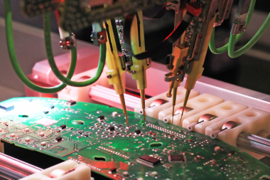
ICT (In-Circuit-Test) equipment is generally used for PCB measurement. It uses Bed-Of-Nails to touch all parts of the board that need to be measured for the test.

A PCB test point is a small loop of wire used to test a probe on a PCB containing surface mount components. They enable users to inject test signals or monitor circuit boards during production. Test sites come in a variety of materials, sizes and colors.

The PCB test point provides a location for the J-hook, or has a sharp tip to contact the conductor on the plate. Most surface mount test sites use phosphor bronze alloys, but they can also be coated with a more affordable silver coating.

What are the advantages of adding test points to your PCB?

Implementing test points in PCB design will provide the following benefits during development:

  • Time and cost savings:

By detecting connection problems through test points in the early design phase, you can save time and money in the later phases.

  • Test convenience:

Test points offer a much lower configuration than other test probe connection types. The shape of the test point is similar to that of the surface mount element, making it a more versatile option.

  • Easy error detection:

Test points simplify the probe testing process, making it easier to detect potential problems.

How to design a PCB with test points?

The following factors should be considered for the correct placement of test points:

  • Board side:

Typically, placing all test points on the same side of the PCB simplifies the testing process, thus saving time and money.

  • Test point distribution:

By evenly distributing test points throughout the PCB, you can test with multiple probes more easily.

  • High Component area:

Specifying PCB areas for high components can also simplify the testing process.

  • Minimum test point distance:

PCB test points should be at least 0.100 inches apart to improve test efficiency.

  • Manufacturing tolerances:

Consider manufacturing tolerances when creating the initial layout of the PCB. During the test phase, the PCB needs space to accommodate the test points and probes.

Choose KingPCB to be your PCB supplier

At KingPCB, whether it is mass production, prototyping, proofing services, we have the confidence to complete any of your PCB manufacturing and assembly needs!

Contact us now for a free quote on your project.

Categories
PCB Blog

What is PCB OUTGASSING?

To ensure that defects are not created during production and use, PCB manufacturers outgassing printed circuit boards during production. Find out what can be done to prevent or reduce outgassing in this article.

What is PCB outgassing?

When outgassing occurs, the gases trapped in the PCB will release within the board in two common situations

During this process, any moisture near the through-hole is turned into vapour by the heat. When this gas escapes, it creates voids in the solder resist layer.

  • Use in ultra-high vacuum environments:

In applications involving ultra-high vacuum environments (such as outer space, laboratories or medical facilities), the vacuum can cause vapour to escape from the PCB, thus creating condensation in the rest of the device.

What are the consequences of PCB outgassing?

Both of these situations occur at different stages of the PCB lifecycle and so present a number of challenges to manufacturers, both of which can lead to defects in the PCB and therefore to a non-functional product.

When outgassing occurs during the soldering process, voids can form in the solder resist layer, which can lead to serious problems. During the deposition process, PCBs need to be drilled and copper plated, with a uniform layer of chemically plated copper acting as a conductor of electricity in the board. Outgassing of PCBs can lead to gaps in the copper plating, which can block the passage of current and cause defects and failures in the PCB.

The problem with outgassing in high vacuum environments depends on the equipment used. In space-related applications, outgassing forms condensate that can interfere with camera lenses or measuring tools, for example, causing problems with measurement results.

Medical facilities and scientific laboratories must have a sterile environment in order to use their equipment properly. Outgassing can contaminate equipment and the surrounding environment, posing a risk to patients or leading to inaccurate test results.

What are the available solutions?

Choosing the right materials

When choosing the materials that make up a PCB, plating made from gold, silver or tin may contain salts or organic substances which can generate gases when heated during the deposition process.

Correct manufacturing

To achieve a high quality PCB then the correct control of the manufacturing process is essential. When the chemical copper plating is too thin or the pre-heating process is incorrect, off-gassing usually occurs during the soldering process.

Even if the PCB has the right material and production method, it can still outgas in high vacuum applications. Baking PCBs for high vacuum systems during production is effective in reducing outgassing, especially when done in vacuum. The baking process removes any residual moisture before use.

Alternatively, when implementing PCBs, customers can design equipment to keep vapours away from critical components. Developing a path for the gas to escape through ventilation holes can prevent it from being trapped.

Choosing the right supplier ensures high quality PCBs

KingPCB is one of the leading PCB manufacturers in China and we have over 15 years of experience in manufacturing, assembly and sourcing of electronic components.

Choose to contact us for any assistance in finding the right PCB for you