Categories
PCB Blog

PCB Wire Harness Fabrication and Assemblies- A Perfect Guide on 2023

Nowadays, people’s life gradually tends to develop electronically and informatization and the demand for electronic products is expanding.

The demand for wire harnesses continues to grow and the market is in high demand. When it comes to making custom electronic wire harnesses and wiring harness assemblies, the details matter greatly.

Here’s everything you need to know about cable assemblies and harnesses.

What are electronics cable and harness assemblies?
Harnesses

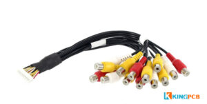
A wire harness consists of multiple wires and a thermoplastic or thermoset external sheath. To put it simply, a wire harness assembly is a processed bundle of wires with a protective sheath.

Because of the nature of the outer jacket, it cannot be used in a wide range of applications in harsh and demanding environments. That is why wire harnesses are used for internal work, such as personal computers or small electronics. Because of their use in small electronics or internal systems, wire harnesses are not as durable as cable assemblies.

Advantages of harness assemblies

  • Optimization of space
  • Customized flexibility
  • Improved equipment safety
  • Increased life of custom cable assemblies and wires

Cable assemblies

In our daily life, you may have noticed some electrical control panels with fuses and sockets, and a whole string of wires and cables connecting different components to that central hub. These wires and cables are all designed to carry electricity and certain signals, and this entire system together has been called a cable assembly.

The sheath of the cable assembly is made of heavy-duty materials that can withstand environmental stresses, and heavier housing is used because the assembly operates in harsher environments. The outer shell of a cable assembly can withstand following situations as below:

  • Wear and tear
  • Extreme temperatures
  • Moisture
  • Compression and expansion

Cable and harness design
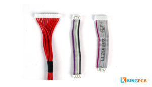
The first and most important step in any electrical manufacturing process is pre-planned design. This also applies to developing cable and harness assemblies.

The wiring harness is the main body of the circuit network, and each circuit in the harness is the basis for its stability. Therefore, in the process of designing the electrical circuit, it is necessary to have high requirements for reliability.

Optimize the number of harness circuits

To perform a function in an electrical system, multiple circuits are usually required. Each circuit in a wiring harness affects the reliability of the entire system, so it can be argued that reducing the number of circuits reduces the chance of failure. But not at the expense of safety, emissions or comfort, etc., but to achieve a reasonable optimization of the system.

Reliability of terminals and connectors

Terminals and connectors are also one of the very important components of the harness, their performance directly determines the overall performance of the harness. Common failures of poor contact, fixed off and poor insulation. Choose the right connector with stable performance to improve the reliability of the wiring harness design.

Design of harness protection

The outer wrap design of the wire harness can play a role of wear resistance, cut resistance, corrosion resistance, etc. For example, for parts with intensive heat generation more area, should choose a high-temperature resistance level of the bellows wrap, such as the engine compartment wiring harness. In short, different wrapping materials should be used according to the specific environment to wrap and protect the wiring harness.

Electronics Prototyping

Prototyping is a common practice in the electronics manufacturing industry. Creating a test version of the final product is critical to resolving any issues that were not addressed during the design phase.

In addition, prototyping gives engineers the opportunity to experience the real thing first hand, which helps them come up with more efficient layouts or refine blueprints.

Harness Production and Assembly

In a broad sense, the steps involved in building a wire harness include

  • Batch cutting the wire to the proper length with a cutter
  • Stripping wire ends and connecting terminals or connectors
  • Gathering the wires into a harness that meets the design specifications
  • Sealing the wire ends

How to Troubleshoot Wire Harnesses and Cable Assemblies?
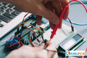
There is no doubt that any kind of product that has problems in situations one can expect and not plan for, cable assemblies and harnesses will also face some failures.

Only through careful analysis of the causes and reasonable testing can we find the cause of the failure and solve it in the right way. Let’s see what causes wiring harness and cable assembly failures and fix them with proper measures.

Common problems with cable assemblies

  • Not choosing the correct cable. The performance of the selected cable assembly is different for different applications. Improperly selected performance that is not durable enough or does not hold up well may lead to product strikes
  • Improper installation. Incorrect soldering work and tooling setup can also affect its performance.
  • Improper testing.

Common problems with wire harness assemblies

  • Improper layout
  • Wire preparation
  • Improper labeling
  • Defects related to soldering
  • Missing components
  • Improper wire tying

Intermittent Errors in Cable Assemblies and Harnesses

Common intermittent errors in cable assemblies and harnesses include open circuits, short circuits, and miswiring.

Possible causes for the above are

  • Improper setup
  • Improper pin contact
  • Worn or dirty contacts
  • Weak contacts

Despite taking a number of steps to avoid errors in cable assemblies and harnesses, errors can still occur. At this point, it is important to thoroughly test the cable assemblies and harnesses. Some common test methods are

Mechanical Performance Testing

Some of the mechanical properties items to be tested include

  • Elongation
  • Tensile strength
  • Flexibility
  • Impact resistance
  • Drop-impact resistance
  • Shrinking
  • Bending force
  • Insulation notch strength

Environmental test

This test is mainly to confirm whether it can withstand environmental conditions

  • Temperature
  • Humidity
  • Vibration
  • Dust, etc.

Electrical test

It mainly involves the following

  • Open wire
  • Improper wiring
  • Risk of short circuit

Visual testing

Ensuring all components are in good condition

  • Wire and cable condition
  • Correctness of connectors
  • Labeling correctness

Signal integrity testing

Signal integrity tests evaluate the signal strength that a cable assembly or harness is able to carry. Some of the factors they look at include signal errors and crosstalk. They also check if signal strength can be maintained by integrating connectors, filters, or splices.

How do you customize your cable and harness?

The important thing to remember is that the more detailed information you provide to the PCB manufacturer, the fewer problems you may face.

  • Detailed images of connectors and pin locations
  • Wire list
  • List of materials
  • Assembly drawings
  • Test specifications

What are the main applications of wire harnesses and cables?
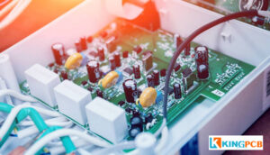
Wire harnesses are one of the fastest-growing and most in-demand electronic components in the industry in today’s electronic and information era.

The function of electronic wiring harnesses has expanded from ordinary signal transmission to data transmission. Wire harnesses have a wide range of applications, from popular household appliances to communications equipment, computers, and external devices. As well as security, solar, aircraft, automotive and military instrumentation are all widely used. In simple terms, any device that needs to be powered by electricity needs to use a wire harness as a transmission medium.

Automotive wiring harnesses

Wire harnesses perform an important role in the operation of automotive systems, such as directional control systems, brake systems, lighting controls, etc. For applications involving safety, the automotive industry has more stringent requirements for wiring harnesses.

Common wiring harness standards are UL/CSA, CCC, VDE, PSE, etc. Currently, the most used are UL/CSA wires.

According to the use of environmental requirements, automotive wiring harnesses try to choose the temperature, oil, wear, water, corrosion, oxidation, flame retardant, and other characteristics.

Technology trends in wire harnesses and cables

As technology continues to evolve, the requirements for convenience, mobility, speed, and power have led to more changes in the equipment we use, leading to the progressive development of electronic products to a higher level. Wire harnesses and cables will undoubtedly have to keep up with them.

The following are a few key technology trends that will have a strong impact on the future of wire harnesses and cables.

Ultra-high bandwidth, lower latency, lower loss

Following the launch of the much-anticipated 5G technology, the facilities carrying its technology will require higher data rates. Highly connected networks have a profound impact on markets such as automotive, transportation, and testing.

Combined user identification pairing

Some of the latest interconnect solutions enable secure, correct pairing of technologies to users through magnetic, LED, or vibration functions, which are particularly important in highly reliable, high-tech applications such as medical, industrial automation, military, and aerospace.

Miniaturization, dense design

Evolving technology has influenced the gradual development of electronic devices in the direction of portability and compactness. The boom in wearable devices has enabled wire harnesses and cable suppliers to offer miniaturized profiles with higher contact densities, providing more flexibility for medical, military, and consumer electronics.

Wireless Power Technology

Wireless power transmission technology has improved the mobility and convenience of electronic devices. It has become a popular feature in smartphones, earbuds, fitness bracelets, PDAs, and other devices, and it is also making its way into electric vehicles. Near Field Communication (NFC) is the newest member of the wireless power standard and has traditionally been used as a communication platform with an installed base of billions of devices.

However, the NFC Forum standards body has turned on a small amount of power transmission (receiving about 0.5 watts) in its protocol. This creates new opportunities for wireless charging in a variety of small, space-constrained devices.

Green Energy

As technology continues to shift to more environmentally friendly green energy technologies, the application of wireless charging technology is escorting it. While wireless charging technologies may wreak havoc on plug-and-play charging stations, they will create other power connector and cable opportunities. In addition, the convenience of wireless charging may serve as a catalyst for the widespread adoption of electric vehicles.

To sum up

Now that you understand the process behind manufacturing custom cable and harness assemblies, proper use of troubleshooting mechanisms and appropriate testing methods ensure that you will not experience performance issues with cable assemblies and harnesses.

If you need access to the custom wire harness and cable assembly services, contact us now for a quick quote, or via email by sales@kingpcb.com

Categories
PCB Blog

Breadboard and PCB – What’s the Difference?

It goes without saying that printed circuit boards are important for electronic devices. PCBs carry various electronic components that provide circuit connections and various complex functions for different devices.

When you learn to create circuits as a beginner, a breadboard would be a good choice.

Breadboards, also known as prototype boards, are solderless boards with one or both sides. Since the board has many small jacks, various electronic components can be inserted or pulled out at will as needed.  Eliminating the need for soldering and saving time in circuit assembly, and the components can be reused, making it ideal for assembly, debugging and training of electronic circuits.

The common specifications of breadboard are 170 holes (35*47mm), 400 holes (85*55mm), 800 holes (165*55mm), etc.

Let’s look at some of the differences between PCB and breadboard

1. Application

Breadboard is suitable for the development stage and can change at will according to the demand. PCB is used for final electronic product integration, manufacturing and assembly according to Gerber files.

2. Components

One obvious difference between breadboard and PCB is that the components on the breadboard do not need to be soldered and can be changed instantly, so it is also called solderless breadboard. While the components on the PCB need to be soldered, such as SMT technology and PTH technology, so the PCB is also relatively more stable.

3. Capacity

There is no doubt that the load-bearing capacity of the PCB is significantly higher than that of the breadboard. Breadboard connects components through wires, so the current-carrying capacity is minimal. At the same time, PCB can also add a variety of components, but in the breadboard can not be completed.

4. Type

Breadboard is rigid, while PCB has a variety of options, it can be rigid, flexible, rigid-flexible combination to meet the needs of different scenarios.

5. Complexity

Even the simplest PCB has a much more complex structure than a breadboard. Usually breadboard consists of distribution bus and holes, PCB’s structure has at least substrate, copper layer, solder resist and screen printing.

6. Function

Breadboard supports components in a mechanical way, it does not perform electrical functions. PCB connects circuits in a mechanical and electrical way.

7. Appearance

The appearance of a breadboard is almost unchanging and relatively homogeneous. Whereas PCBs can be customized in various shapes, colors.

Choosing breadboards or PCBs?

If you are a circuit enthusiast or a beginner, breadboard can meet your needs. Breadboards can be easily prototyped and are relatively inexpensive. If you are looking for a long term, feature rich device, then a PCB is obviously the best choice.

Do you want to turn your breadboard prototype into a PCB?

After you have completed your development testing, you need to generate the Gerber files and Bom list for manufacturing your PCB.  Then send these files to a professional PCB manufacturer, such as KingPCB, and we will carefully review your files and provide a quick quote, and then you can produce and assemble your PCB.

If you have any questions or want to get more information about PCB manufacturing, contact us now or send emails at sales@kingpcb.com
Categories
PCB Blog

Eight Tips for Beneficial PCB Assembly

Are you working on your project prototype and ready to go into production? Here are some tips for PCB assembly that can help you better complete your project.

Favorable PCB assembly Tips

1. Effective communication

There is nothing better than efficient communication. Clear communication with your PCB manufacturer can greatly reduce the PCB production cycle time.

Make sure everything is communicated clearly and unambiguously, and that each part’s markers, polarity markings, etc. are worthy of your attention.

In fact, working with a reliable PCB supplier can be a great resource for you, especially when it comes to introducing you to new product technologies, industry best practices, and more.

2. PCB structure

To ensure that you don’t encounter problems during PCB assembly, it’s important to adhere to tried-and-true standards.

3. Optimize PCB production costs

It is best to look for ways to optimize production costs as early as possible. PCB production costs are controlled through a variety of effective measures, however, it is important to weigh the pros and cons associated with each decision. You need to keep in mind that there are risks associated with sub-standard parts, as this can not only offset cost advantages, but also prove risky in terms of company reputation. Another aspect to keep in mind is the delay in timely delivery, as this can also have costly consequences.

4. Naming

The labeling of the components in the design should not be overlooked either. Make sure that all components in the design are properly labeled and that they are numbered as well. Avoid problems due to naming differences.

5. Component Interchangeability

It is best to choose parts that are readily available to avoid wasting valuable time.

6. PCB board size

Improving board efficiency requires you to stick to standard board sizes whenever possible. A larger board will be easier to route, but it also means increased costs; a smaller board may be easier to check, but it may cost more due to the extra layers.

7. PCB manufacturing thermal issues

Pay attention to the thermal balance in the PCB. For example, the placement of components, placing large parts next to small parts may have thermal problems.

8. Check the files

Finally it is also important to double check all the files before sending them to your PCB supplier to make sure they are the latest version.

To summarize

The above 8 tips can help to some extent to complete your PCB project assembly, so that you do not have to consume extra money and effort.

KingPCB, as one of the leading PCB suppliers in the industry, has more than 15 years of professional experience. We have rich experience in manufacturing and assembling single-layer, double-sided and multi-layer boards.

If you have any questions or requests about PCB assembly services, please feel free to contact us via email at sales@kingpcb.com.


Categories
PCB Blog

Quickly Build New Products By Using PCB Assembly Prototypes

What is PCB Assembly Prototyping?

PCB assembly prototyping is the trial production of circuit boards before mass production.

It mainly applied to electronic engineers in the design of the circuit, and complete the PCB Layout, to the reliable PCBA manufacturer for small batch PCB trial production process.

That is, the rapid prototyping of circuit boards. General engineers in the product design is not completed to confirm and complete testing before, are called PCB prototyping.

What do I need to check for PCB prototyping?

Before you choose a PCB assembly service, it is important to have a clear understanding of your project requirements.

Knowing all production requirements in advance will help you narrow down your search and find the right assembly service for your project.

Prototyping needs to confirm a few basic parameters

1, Board material.

2, Finished plate thickness.

3, Copper thickness.

2, Number of layers.

3, Hole diameter

4, Plating

5, Solder resist layer.

6, Surface treatment process

7, Character

What files are required for PCB prototyping?

Among the documents required for assembly, the most important are Gerber/ODB++, coordinate files, assembly drawings, and BOMs. As a PCB design engineer, if you do not communicate the necessary information to your contract manufacturer (CM) through these documents, a number of errors may occur. These include mismatched component counts, missing pin 1 and polarity markings, missing orientation indicators, packages, etc.

Make sure the Gerber file and BOM file are accurate, replace components with long lead times with components that can be ordered and picked up immediately, because sampling is only a preliminary verification of product design, so you can use alternative materials to save sampling time, or have a long lead time with the supplier before sampling, and then pick up the materials directly when you want to sample, this is also a way to reduce This is also a common method to reduce the waiting time for materials.

PCB & PCBA Fabrication Process:

place order → confirm production information → procurement→ inspection→ production → verification (pics)

Place order

Customers place orders according to their actual needs PCBA processing factory, and put forward specific requirements. And the processing factory will evaluate by their own ability to see if they can complete the order.

Confirm production information

After the customer decides to place an order, he will provide a series of documents and lists to the PCBA processing factory, such as PCB electronic files, coordinate files and BOM lists, etc., which are required for production.

Procurement of raw materials

PCBA fabrication factory according to the documents provided by the customer to the designated suppliers to purchase the relevant raw materials.

Incoming Material Inspection

Before PCB & PCBA processing, all raw materials to be used are subject to strict quality inspection to ensure that they are qualified and put into production.

PCBA production

In the time of PCB & PCBA processing, in order to ensure the quality of production, whether SMD or welding production, manufacturers need to strictly control the furnace temperature.

PCBA testing

PCBA processing factory for strict product testing, through the test PCB board delivery to customers.

Packaging after-sales

Factors Affecting the PCBs Cost

  • Material selection:

The price diversity caused by the different materials used in PCB, board material generally FR-4, CEM-3, etc., board thickness, copper thickness will cause huge differences.

  • Production process:

Different production process costs are also different. For example, sink gold board and OSP, gold plating surface treatment process; solder resist layer ink, ordinary heat-set oil and photopolymer green oil; production shape of the gong board and beer board; the use of silk screen lines and dry film lines, etc. will also affect the price of prototyping

  • PCB design:

Different designs will have different problems. For example, two kinds of circuit boards with different apertures, line width spacing will also have different production costs; for example, a panel with more than 4, 5 different designs, the complexity of the machine in the gong board will become higher, the difficulty of the higher scrap rate, the inevitable cost increases.

  • Customer requirements:

The level of customer requirements will directly affect the board factory’s yield, such as a board by ipc-a-600e, class1 requirements have 98% pass rate, but by class3 requirements may only 90% pass rate.

  • PCB manufacturers capacity:

Even if the same product, but because of different manufacturers process equipment, technology level is different, will also form different costs.

Explore KingPCB’s PCB prototyping services

KingPCB engaged in the electronics industry for more than 20 years of experience, professional and efficient team is committed to providing customers with the best PCB one-stop procurement, assembly, manufacturing services for industrial, consumer electronics, aviation, medical, automotive and other fields.

Contact us now for your project with quick quotation!

Categories
PCB Blog

Why is a PCB Assembly Quote Important for Your PCB Project?

After completing your PCB design, the next step is to choose the right PCB supplier to bring your design to life.

So as a first step, it is crucial to request a PCB quote. To get an accurate quote, be sure to provide your PCB supplier with relevant information about your project.

In general, a PCB assembly service quote contains the following components.

PCB assembly service quote

In simple terms, a standard PCB assembly service quote contains two parts, one is the cost of manufacturing the board, and the second is the price of PCB assembly.

Before requesting an accurate quote, you should provide as much of this important information as possible to ensure that the price and run time estimates:

Documents required for PCB assembly quotation

Accurate quotation depends on the availability of the following documents.

Bare board printing or manufacturing drawings

It provides mainly the following information.

In addition to this, you will need to provide Gerber files, preferably in 274-x format.

Bill of materials

BOM (Bill of materials) is another important document, the more detailed it is, the better for the PCB supplier to estimate the price. The BOM sheet mainly contains information such as part description, number, reference mark, etc.

Assembly print

With assembly printing, information about the location of the parts can be conveyed.

Supplier list

Ideally a list of approved suppliers and the manufacturer’s part number can be provided.

Information often missed when requesting a quote for PCB assembly

The following is some of the information that is often omitted

Stacking

Include the number of layers, thickness, and details related to the lamination

Solder resist

Soldermask type

Impedance

For high-speed PCB manufacturing, impedance details are essential

Depanelization method

The size and location of the cutout is essential to get an accurate quote for PCB assembly

Silkscreen

Silkscreen files and color selection are also essential details

Surface finish

The type of surface finish has a significant impact on the cost

The main factors affecting the cost of PCB assembly

Mounting technology

The use of SMT (surface mount technology) or through-hole assembly will affect the cost. Compared to through-hole assembly surface mount technology is faster and more automated.

Number of layers

The cost of assembling multi-layer PCBs usually requires higher technology, so the cost is also higher.

Surface finish

As mentioned earlier, the choice of surface finish has a significant impact on cost. Some surface finishes have longer shelf life and higher cost.

Delivery time

Usually delivery time and PCB assembly cost is inversely proportional

Shipping costs

High volume PCB production means more packaging, more volume, and more shipping costs.

Explore KingPCB’s PCB assembly services

PCB assembly quotes depend on many factors, and it is important to provide us with detailed information in order to give you an accurate quote. While price is not a deciding factor in choosing a particular supplier, professionalism can be seen in a detailed and professional quotation form.

KingPCB offers reliable, high quality PCB manufacturing and assembly services, contact us now to get a quote for any type of fast PCB assembly service.

Categories
PCB Blog

Why Via Tenting is Important in PCB Manufacturing?

If you have ordered and used PCBs, you have probably heard of the use of vias in printed circuit boards. Vias play an important role in the connections between the layers of the board, and they serve two main purposes.

  • Electrical signal conduction
  • Heat dissipation

In many cases, the through-hole is copper-plated. Some PCB manufacturers believe that these holes should not be exposed, when the vias are completely covered, called filled vias. There is another popular method of tenting vias.

What is PCB Via Tenting?

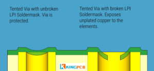
As the name implies, tenting vias means creating a tent-like shape on the vias. Tenting a vias means covering the toroid and vias with a solder resist layer, primarily covering the toroid to prevent exposure to components and reduce accidental shorts or contact with the circuit. Whether to use tenting in PCB manufacturing depends on the design of the board.

Why is PCB Via Tenting important in PCB manufacturing?

There are several ways to protect printed circuit boards from vias. For cost reasons, tented vias are usually preferable to epoxy filling. Most forms of tenting are LPI (liquid imagerable solder resist). PCB solder resist protects copper traces from oxidation, damage and solder bridging, which also applies to over-hole protection.

If your PCB is designed with a through-hole assembly, the tent through-hole will prevent solder from flowing up into the through-hole and over the other side of the PCB when using wave soldering.

The vias near the SMT pad should also be tented. This will prevent the solder paste wick from sucking into the via hole and creating a bad solder joint.

Disadvantages of PCB Via Tenting

Since the LPI solder resist is a liquid, it must “bridge” the gap above the via. This results in the solder resist not completely covering the via, leaving a small hole.

These small holes can be used for corrosive fluxes, moisture and other chemicals to enter the vias. This can lead to failure due to corrosive vias.

This is not an issue due to the popularity of no-clean flux in SMT assembly, but corrosive water-clean flux is still prevalent in through-hole assembly.

Under what circumstances is PCB Via Tenting used?

Whether to use Tenting depends firstly on the PCB design, and secondly on the size of the via.

Tenting vias are suitable for through-hole diameters of 12 mil or smaller. If you are dealing with larger vias, using filled vias is a better option, it is relatively more costly.

Contact KingPCB for PCBs with tented or non-tented vias

At KingPCB, we have experience with almost all types of printed circuit boards. We can help you find boards in a variety of materials, in flexible or rigid-flexible formulations, with tented vias, filled vias, blocked vias, open vias, or a combination of these.

Our high quality manufacturing, ability to deliver, and quick response sets us apart!

Contact us now to get more information about our PCB manufacturing capabilities!

Categories
PCB Blog

Key Factors Affect the Cost of Multilayer PCB Assembly

The application of multilayer PCBs is becoming more and more common.

There are many factors that determine the cost of manufacturing multilayer PCBs, which are mainly divided into the following categories.

  • Material
  • Size
  • Number of layers
  • PCB thickness
  • Surface treatment process
  • Hole type and number
  • Alignment width and spacing
  • Other special process requirements

Materials

The choice of what material to manufacture PCBs has a significant impact on the cost, in the selection of substrates for multilayer PCBs, here are a few points to consider.

  • High and low temperature requirements. For boards that need to operate under high temperature conditions, the need to use high TG material (TG that is, the glass transition temperature point)
  • Signal performance. The choice of material depends on the advantage of being able to provide uninterrupted electrical signals.
  • Mechanical properties.

Size

PCB costs are calculated by size, so the larger the PCB size, the more material required and the cost will increase. But this does not mean that the smaller the size of the cost is less, the processing time involved in small size PCB will also affect the cost.

Number of layers

The number of layers is another major determinant of the cost of multilayer PCBs. For the more layers of PCBs, the more resources and time required for the manufacturing process, the higher the cost.

PCB thickness

PCB conventional thickness is 1.6mm, for thicker materials are usually more expensive in production, lamination and PCB made.

Surface treatment process

The choice of surface finish treatment is critical to improving PCB reliability and shelf life, KingPCB default PCB manufacturing surface treatment is HASL, when it comes to HDI PCB, ENIG may be required, which also has an impact on the cost.

Hole type and quantity

The price of multilayer PCB manufacturing is closely related to the through hole

  • Hole size (conventional holes greater than or equal to 0.3mm)
  • Hole type (whether it involves micro vias, blind vias, buried vias)
  • Quantity (general hole density is not greater than 100000/㎡)

Alignment width and spacing

Multilayer board needs better heat dissipation ability, in order to avoid overheating, need to have enough alignment width. If you expand the alignment width or add extra solder, it will increase the material cost and workload.

Other special process requirements

Some other factors that may affect the cost are impedance control, ink, depth control, halogen-free materials, ink plugging, copper thickness, etc.

Explore KingPCB’s multilayer PCB assembly services

There are many factors that affect multilayer PCB manufacturing and assembly, please be careful when making any budget decision for multilayer PCB assembly.

KingPCB, one of the leading PCB manufacturers in China, uses modern technology and advanced equipment to provide you with PCB assembly services.

If you are looking for a multilayer PCB manufacturer or would like to see a quote for your project, contact us now for a quick quote!

Categories
PCB Blog

Wave Soldering and Reflow Soldering: Which is Better for PCB Assembly

Soldering is an important part of the printed circuit board manufacturing process. The reliability of a circuit board is achieved by sticking electronic components to your board through soldering. Wave soldering and reflow soldering are common soldering methods for PCB assembly.

Each method has its advantages and disadvantages, and this article will walk you through their meaning and application.

What is wave soldering?

Wave soldering is a batch soldering process that allows many boards to be manufactured in a very short period of time.

It is called “wave soldering” because the soldering surface of the plug-in board is in direct contact with the high-temperature liquid tin, which maintains a sloping surface, and a special device makes the liquid tin form a wave-like phenomenon.

Wave soldering process

  • Insert the component into the corresponding hole
  • Pre-application of flux
  • Preheat (90-100 ℃)
  • Wave soldering (220-240 ℃)
  • Cooling
  • Cut off excess plug-in pins
  • Inspection

During the wave soldering process, it is worth noting that proper temperature is very important. Failure to adequately control the temperature may result in cracking and electrical loss.

Wave Soldering Disadvantages

  • Solder consumption
  • Flux consumption
  • Nitrogen consumption
  • Power consumption
  • Need for solder rework after wave soldering
  • Need to clean wave solder holes and solder components

What is reflow soldering?

Reflow soldering is different from wave soldering and is commonly used to solder surface mount components. It is refers to the use of solder paste (a mixture of solder and flux) to connect one or more electronic components to a contact pad and then melt the solder by controlled heating to achieve a permanent bond.

Reflow soldering process flow.

  • Apply pre-solder paste
  • SMT (manual or automatic machine placement)
  • Reflow soldering
  • Inspection and electrical test

Wave vs. reflow soldering

The choice of which type of soldering to use depends on a variety of factors, such as pad shape, component orientation, PCB type, etc.

For printed circuit boards with through-hole components and larger surface mount components, wave soldering is an ideal method.

However, in some ways, wave soldering is more complex and requires careful monitoring of issues such as board temperature and the time the board spends in the solder wave. Failure to create the correct wave soldering environment is more likely to result in board defects.

When using reflow soldering to manufacture printed circuit boards, you don’t need to worry about controlling the environment.

To sum up, wave soldering is faster, cheaper, and cost-effective for high-volume orders. Reflow soldering is typically used for small-scale manufacturing products that do not require a method suitable for fast, inexpensive mass production.

Explore KingPCB’s PCB assembly services

The type of soldering is just one of the many elements of PCB assembly. Choose your soldering partner wisely, research carefully for your requirements and provide a soldering process that works for you.

KingPCB is very knowledgeable about solder types and other elements of PCBs, such as types of substrate materials, board variations, and important design features.

To learn more about KingPCB’s fabrication and assembly information, contact us now!

Categories
PCB Blog

OEM PCB Manufacturer Box Build Assembly Services

PCB box build assembly is very beneficial when producing electromechanical devices. You will see many advantages when you choose a PCB manufacturer that is reliable and has extensive manufacturing experience. They help you to reduce your production costs without causing any defects to your product.

What is PCB box build?

Also known as system integration, a boxed build is a combination of circuit boards, cables and wires, subassemblies, and finally, case fabrication.

Once it is fully completed, the assembly is a finished product that operates as intended with a practical enclosure that meets the needs of the application.

The process of PCB box assembly involves

  • Fabrication of the PCB
  • Assembly of the PCB
  • Connection of component wires and cables

Choosing the right enclosure is critical to the success of your electronic equipment, whether it is part of a wireless industrial control, medical device, or energy distribution system.

PCB Box Build Design Guidelines and Best Practices

Proper box build design will ensure the long-term success of your electronics project. Once you have identified your electronics contract manufacturer, you must provide them with a variety of information to continue your work. You should provide them with all the essential information they may need.

The strategy for PCB box builds can be boiled down to

  • Size
  • Material
  • Transmission
  • Layout
  • Compatibility
  • Testing requirements


Confirm proper dimensions

Use 3D modeling to create a perfect-fitting enclosure. Size is an important part of the final product, and the size and weight of the product will be one of the most important factors affecting shipping costs.

  • Packaging
  • Shipping
  • Storage

As a general rule, it is more difficult to build the right enclosure if the device is larger. Work with your product development team to ensure that the size of your equipment meets manufacturability design requirements.

Select the right enclosure material

When building for a PCB box, consider the following factors when selecting the right material.

  • Durability
  • Ductility
  • Usability
  • Cost
  • Application requirements: environmental factors

Ensure adequate signal transmission

Metal enclosures may impede the transmission of wireless signals. Plastic enclosures are more suitable for wireless devices, but when used in extreme temperature environments, metal enclosures are still preferable.

Choose a thoughtful layout and design

In understanding the audience of your product, consider the brand theme of the product to design the appearance of the product.

Compare CAD with BOM

Compare your CAD with the BOM (Bill of Materials) before going into production to ensure package compatibility. The bill of materials is like a blueprint for PCB boxed assemblies, which provides information on

  • Package
  • Reference number
  • Item number
  • Part type
  • Manufacturer part number, etc.

Test Requirements

You must inform the PCB manufacturer of your requirements for product testing; you can also ask your PCB supplier for available test methods first. The conventional test methods are

  • Functional testing
  • Basic electrical testing
  • Aging testing

Why choose PCB box build assembly service?

Success with PCB box build assembly services can be achieved in a number of ways. PCB box build services help integrate PCB systems in two different ways: the fabrication of the PCB and the installation and its wire connections.

Providing detailed information about your manufacturing requirements to your PCB partner ensures your success with PCB box builds.

Explore KingPCB’s box build services

As one of the leading PCB manufacturers in China, KingPCB offers customized PCB electronics box build and system assembly services with advanced technology. Request a Box Build Assembly quote contact us now!

Categories
PCB Blog

Which Works better? Thermal Pad vs. Thermal Paste?

With the miniaturization and intensification of electronic products, how to effectively dissipate heat has become a matter that PCB manufacturers need to face.

Thermal Analysis

Effective thermal management requires a detailed thermal analysis.

Thermal analysis assists designers in determining the electrical performance and reliability of components on the PCB, helping to determine whether components or PCBs will fail or burn out due to over-temperature function.

A simple thermal analysis simply calculates the average temperature of the PCB, while a complex one models the transients of electronic devices containing multiple PCBs and thousands of components.

PCB thermal management design practices

There are several thermal methods that can be used when designing and prototyping PCBs.

To ensure a good connection between the IC and the heat sink, thermal pads and thermal paste are often used.

What are thermal pads and paste?

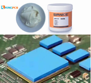
Thermal pad

Thermally conductive pads are made of thermally conductive materials that are inherently sticky, soft, good compression properties, and excellent thermal conductivity. They help to dissipate heat easily when placed between the component and the heat sink.

What are the advantages of thermally conductive pads?

  • Easy deployment
  • Flexibility to cut to any size
  • Multiple material options

Thermal Paste

Essentially, thermal paste performs the same function as a thermal pad. The thermal paste works by closing any air gap between the heat generating component and the heat sink. This ensures that the air gap does not act as a thermal insulator and that heat is easily dissipated.

What are the advantages of thermal conductive paste?

  • Price advantage
  • Easy to apply, fills uneven gaps and provides a thinner interface, thus providing better thermal conductivity
  • Durable and more robust

Choose thermal pad or thermal paste? Which works better

The truth is that no one choice is absolutely perfect. Each material has its advantages and disadvantages, and the choice depends on the application requirements of the product. All we need to do is to carefully evaluate the thermal requirements of the board and then choose the most suitable material.

In addition to using thermal pads or thermal paste, you also need to use appropriate through-hole and surface mount pads, alignment wiring, and power layers for your IC design. This will greatly help you to manage the thermal condition of the board.

Explore KingPCB’s manufacturing services

In essence, thermal management is a technique used by PCB manufacturers.

KingPCB as one of the leading PCB manufacturers in China has over 10 years of experience. It is our goal to adhere to strict high standards of PCB manufacturing and assembly.

To get a fast PCB manufacturing quote, contact us now!

Categories
PCB Blog

Common Errors and Solutions in SMT PCB Assembly

Surface mount technology is one of the most popular technologies and processes in the electronics assembly industry. When SMD assembly of printed circuit boards, SMT may lead to some PCB failures, reduce and avoid these defects to help improve the efficiency of PCB assembly services.

First of all, let’s review the knowledge related to SMT

What is surface mount technology?

Surface mount technology is a process of mounting electronic components directly onto the surface of a printed circuit board. The electronic components mounted in this way are called surface mount devices (SMD)

What are the advantages of surface mount technology?

Compared to PTH, SMT makes automation and higher density components on the board easier and allows for higher circuit speeds and better frequency performance.

What are the surface mount technology failures?

 Bridging

Solder bridging errors can lead to electrical shorts, which can cause circuits to malfunction.

  • Causes: The most commonly recognized causes make problems in the solder paste printing process, deviations in PCB pad configuration or stencil layout. Excessive solder paste deposition and solder paste cold collapse rate can also lead to bridging.
  • Solution: Select the proper solder paste metal to flux weight ratio, in other words, the solder paste will not collapse. Set the proper reflow profile, ensure point pressure and accuracy of component placement, etc.

Insufficient solder joints or electrical open circuits

When two electrical connection points are separated or the PCB breaks the circuit is called an electrical open circuit

  • Causes:Insufficient solder on the connector or solder paste blocking the holes of the stencil, or sufficient amount of solder paste, but in the reflow device does not contact with both the leads and pads
  • Solution: First, you can correct the stencil aspect ratio, the aspect ratio is too small may lead to solder paste blocking the hole. Also control the environmental conditions to avoid solder paste contamination.

Solder balls

Solder ball particles can form a false bridge between two adjacent leads, thus causing functional problems to the circuit.

  • Causes: One of the main causes of solder balls is when the solder paste is contaminated with moisture. Excessive oxides of solder powder in the solder paste will also form solder balls.
  • Solution: You can choose a coarser powder size

Tombstone

Tombstone defect is the component warped from the pad, or perpendicular to the board

  • Cause: It is caused by unbalanced force during reflow soldering. There is also uneven heating resulting in differences between component terminals.
  • Solution: The component body must cover at least 50% of the two pads to avoid unbalanced soldering forces. It is recommended to maintain a high preheat temperature so that the difference between the two ends during reflow is reduced.

Non-wetting or de-wetting

Non-wetting is defined as the inability of the molten solder to form a metallic bond with the base metal. The result is that the PCB pads or terminals of the assembly do not capture the solder during reflow.

De-wetting usually refers to alloy solder joints that do not extend to the PCB pads, so they do not get a good solder joint weld.

  • Causes: Poor PCB finish, too long soaking time during reflow, insufficient heat and other reasons.
  • Solution: Adjust the metal surface finish, such as higher temperature resistance OSP or ENIG. reduce the total analysis time before the reflow stage.

Solder beads

Solder beads are different from solder balls in that they are discrete.

  • Causes: Excessive solder paste; sometimes flux abandonment exceeds the coagulation force of solder paste during the preheat stage.
  • Solution: Reduce the thickness of the stencil or reduce the size of the aperture to reduce component pickup and placement pressure.

Insufficient filling or insufficient solder paste

The amount of solder paste deposits during printing is too small or there is insufficient solder after reflow to form round corners at the component leads.

  • Causes: Solder paste annual or metal content is too low; squeegee speed is too fast; stencil is sometimes clogged by dried paste, etc.
  • Solution: Clean the stencil regularly and control the speed of the scraper not too fast

Cold soldering or granular joints

PCBA solder end of the paste is not fully melting back to the phenomenon. For example, there are granular solder joints, the surface of the solder joint is not smooth irregular shape, or metal powder completely melted.

  • Causes: Reflow temperature is too low resulting in insufficient heat absorption of the solder, or reflow time is too short, or PCB pad cleaning is not sufficient and other reasons.
  • Solution: The maximum reflow temperature should be high enough; do not move the component during or after reflow; alloy analysis is necessary to check for the presence of contaminants.

Explore KingPCB’s SMT services

As PCBs miniaturize, more stringent and precise soldering control of the PCB assembly process is necessary. Reducing common errors in SMT is beneficial to improve SMT manufacturing efficiency.

KingPCB, as one of the leading PCB suppliers in China, has over 10 years of extensive manufacturing and assembly experience for your PCB project, contact us today for more information about our PCB services.